This thread has been locked.

If you have a related question, please click the "Ask a related question" button in the top right corner. The newly created question will be automatically linked to this question.

TM4C1294NCPDT: ADC analog signals: AIN16-19 (IO PK1-3) not working in software

Part Number: TM4C1294NCPDT

Tool/software:

Hi,

I configured the ADC analog inputs as follow:

ROM_GPIOPinTypeADC(GPIO_PORTK_BASE, GPIO_PIN_0);   // AIN16

ROM_GPIOPinTypeADC(GPIO_PORTK_BASE, GPIO_PIN_1);   // AIN17

ROM_GPIOPinTypeADC(GPIO_PORTK_BASE, GPIO_PIN_2);   // AIN18

ROM_GPIOPinTypeADC(GPIO_PORTK_BASE, GPIO_PIN_3);   // AIN19

and then try to read the value from it:

ADCSequenceConfigure(ADC0_BASE, 3, ADC_TRIGGER_PROCESSOR, 0);

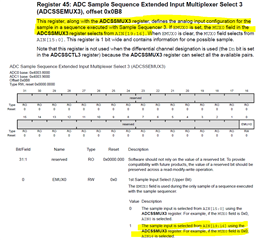
ADCSequenceStepConfigure(ADC0_BASE, 3, 0, ADC_CTL_CH16 | ADC_CTL_IE |
ADC_CTL_END);                                                                                                                        // and so on for ADC_CTL_CH17/18/19


//
// Since sample sequence 3 is now configured, it must be enabled.
//
ADCSequenceEnable(ADC0_BASE, 3);

//
// Clear the interrupt status flag. This is done to make sure the
// interrupt flag is cleared before we sample.
//
ADCIntClear(ADC0_BASE, 3);

//
// Sample the temperature sensor forever. Display the value on the
// console.
//
while(1)
{
//
// Trigger the ADC conversion.
//
ADCProcessorTrigger(ADC0_BASE, 3);

//
// Wait for conversion to be completed.
//
while(!ADCIntStatus(ADC0_BASE, 3, false))
{
}

//
// Clear the ADC interrupt flag.
//
ADCIntClear(ADC0_BASE, 3);

//
// Read ADC Value.
//
ADCSequenceDataGet(ADC0_BASE, 3, ADCValues);

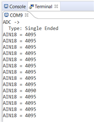
The other AIN0-15 are working just fine, and I can read their values.

the HW-engineer that works with me was able to touch the Pins (18-21 accordingly) and to see the wanted value. 

Any help will be appreciated,

Tzipi

  • Hi,

      Can you elaborate what is not working with AIN16-AIN19? Is it that you are reading random values or what has actually happened? Can you read ADCSSEMUX3 and ADCSSMUX3 registers? I just wanted to know if you are muxing in AIN[19:16]. 

  • Hi Charles,

    Thank you for your response.

    I am reading random values from AIN16-19.

    I read registers ADCSSEMUX3 and ADCSSMUX3 while debugging my code and the value is 0 for both of them.

    so, I understand that I need to set ADCSSEMUX3 register to 1 before I go and read AIN16-19. 

    I don't know how to set it, can you please help? which function should I use to do so?

    Is there anything else I need to do before readding AIN16-19 values?

    Thank you,

    Tzipi

  • Hi,

     Can you try to write to ADCSSEMUX3 manually using HWREG() function? I'm currently on travel. I can show a example of using HWREG later today if you need. 

  • I will try it and update you here, Thanks!

  • Hi Charles,

    I succeed to write ADCSSEMUX3 with HWREG() function. 

    If I do so before all the above code - it doesn't change the reading values of AIN16-19 - it just like before: reading some random values and AIN17-19 got the same value while they should be different... (it was like this also before doing the HWREG() function).

    If I do so before the ADCSequenceDataGet function I read zeros.

    I noticed the comment in the page you sent me from the datasheet that says: 

    what does it mean?

    the value of the register ADCSSCTL3 is 0x00000007 during the runtime.

  • Hi Tzipi,

      Sorry that I just got back from my travel. I run the below code for AIN18 with PK2 tied to 3.3V on the LaunchPad. I can see it convert to 4096. Please find below and can you please try it too?

    #include <stdbool.h>
    #include <stdint.h>
    #include "inc/hw_memmap.h"
    #include "driverlib/adc.h"
    #include "driverlib/gpio.h"
    #include "driverlib/pin_map.h"
    #include "driverlib/sysctl.h"
    #include "driverlib/uart.h"
    #include "utils/uartstdio.h"
    
    //*****************************************************************************
    //
    //! \addtogroup adc_examples_list
    //! <h1>Single Ended ADC (single_ended)</h1>
    //!
    //! This example shows how to setup ADC0 as a single ended input and take a
    //! single sample on AIN18/PK2.
    //!
    //! This example uses the following peripherals and I/O signals.  You must
    //! review these and change as needed for your own board:
    //! - ADC0 peripheral
    //! - GPIO Port E peripheral (for AIN18 pin)
    //! - AIN18 - PK2
    //!
    //! The following UART signals are configured only for displaying console
    //! messages for this example.  These are not required for operation of the
    //! ADC.
    //! - UART0 peripheral
    //! - GPIO Port A peripheral (for UART0 pins)
    //! - UART0RX - PA0
    //! - UART0TX - PA1
    //!
    //! This example uses the following interrupt handlers.  To use this example
    //! in your own application you must add these interrupt handlers to your
    //! vector table.
    //! - None.
    //
    //*****************************************************************************
    #define USER_LED1  GPIO_PIN_2
    
    #define SEQNUM 3
    //*****************************************************************************
    //
    // This function sets up UART0 to be used for a console to display information
    // as the example is running.
    //
    //*****************************************************************************
    void
    InitConsole(void)
    {
        //
        // Enable GPIO port A which is used for UART0 pins.
        // TODO: change this to whichever GPIO port you are using.
        //
        SysCtlPeripheralEnable(SYSCTL_PERIPH_GPIOA);
    
        //
        // Configure the pin muxing for UART0 functions on port A0 and A1.
        // This step is not necessary if your part does not support pin muxing.
        // TODO: change this to select the port/pin you are using.
        //
        GPIOPinConfigure(GPIO_PA0_U0RX);
        GPIOPinConfigure(GPIO_PA1_U0TX);
    
        //
        // Enable UART0 so that we can configure the clock.
        //
        SysCtlPeripheralEnable(SYSCTL_PERIPH_UART0);
    
        //
        // Use the internal 16MHz oscillator as the UART clock source.
        //
        UARTClockSourceSet(UART0_BASE, UART_CLOCK_SYSTEM);
    
        //
        // Select the alternate (UART) function for these pins.
        // TODO: change this to select the port/pin you are using.
        //
        GPIOPinTypeUART(GPIO_PORTA_BASE, GPIO_PIN_0 | GPIO_PIN_1);
    
        //
        // Initialize the UART for console I/O.
        //
        UARTStdioConfig(0, 115200, 120000000);
    }
    
    //*****************************************************************************
    //
    // Configure ADC0 for a single-ended input and a single sample.  Once the
    // sample is ready, an interrupt flag will be set.  Using a polling method,
    // the data will be read then displayed on the console via UART0.
    //
    //*****************************************************************************
    int
    main(void)
    {
        uint32_t ui32SysClock;
    
        //
        // This array is used for storing the data read from the ADC FIFO.
        //
        uint32_t pui32ADC0Value[0];
    
        //
        // Set the clocking to run at 20 MHz (200 MHz / 10) using the PLL.  When
        // using the ADC, you must either use the PLL or supply a 16 MHz clock
        // source.
        // TODO: The SYSCTL_XTAL_ value must be changed to match the value of the
        // crystal on your board.
        //
    
        ui32SysClock = SysCtlClockFreqSet((SYSCTL_XTAL_25MHZ |
                                           SYSCTL_OSC_MAIN |
                                           SYSCTL_USE_PLL |
                                           SYSCTL_CFG_VCO_240), 120000000);
    
        //
        // Set up the serial console to use for displaying messages.  This is
        // just for this example program and is not needed for ADC operation.
        //
        InitConsole();
    
        //
        // Display the setup on the console.
        //
        UARTprintf("ADC ->\n");
        UARTprintf("  Type: Single Ended\n");
    
        //
        // The ADC0 peripheral must be enabled for use.
        //
        SysCtlPeripheralEnable(SYSCTL_PERIPH_ADC0);
    
        SysCtlPeripheralEnable(SYSCTL_PERIPH_GPIOK);
    
        /*
         * ADC Clock runs at 30Mhz
         */
    //    ADCClockConfigSet(ADC0_BASE, ADC_CLOCK_SRC_PLL, 10);
    
    
        /* PK2 - AIN18
         */
    
        GPIOPinTypeADC(GPIO_PORTK_BASE, GPIO_PIN_2 );
    
        ADCSequenceConfigure(ADC0_BASE, SEQNUM, ADC_TRIGGER_PROCESSOR, 0);
    
        ADCSequenceStepConfigure(ADC0_BASE, SEQNUM, 0, ADC_CTL_CH18 | ADC_CTL_IE |
                                 ADC_CTL_END);
    
        ADCSequenceEnable(ADC0_BASE, SEQNUM);
    
        ADCIntClear(ADC0_BASE, SEQNUM);
    
        while(1)
        {
    
    
            //
            // Trigger the ADC conversion.
            //
    
            ADCProcessorTrigger(ADC0_BASE, SEQNUM);
    
            //
            // Wait for conversion to be completed.
            //
            while(!ADCIntStatus(ADC0_BASE, SEQNUM, false))
            {
            }
    
            //
            // Clear the ADC interrupt flag.
            //
            ADCIntClear(ADC0_BASE, SEQNUM);
    
            //
            // Read ADC Value.
            //
            ADCSequenceDataGet(ADC0_BASE, SEQNUM, pui32ADC0Value);
    
            //
            // Display the AIN18 (PK2) digital value on the console.
            //
            UARTprintf("AIN18 = %4d\n", pui32ADC0Value[0]);
    
            //
            // This function provides a means of generating a constant length
            // delay.  The function delay (in cycles) = 3 * parameter.  Delay
            // 250ms arbitrarily.
            //
    
            SysCtlDelay(ui32SysClock / 100);
    
        }
    }
    

    For the above code I use, Sample Sequence 3 is used. Below are the register settings pertaining to SS3. 

  • i found my mistake! thank you!!