Part Number: AM2432
Other Parts Discussed in Thread: SYSCONFIG
Tool/software:
Hi all:
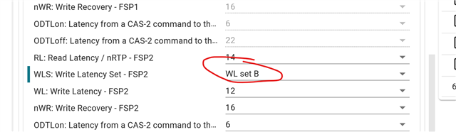
Our project uses AM2432 with LPDDR4 external RAM model IS43LQ32256B-062BLI&ISSI. Recently, during testing DDR timing, we found that the phase relationship between DQS and DQ does not comply with the DDR manual when SOC writes to DDR. Could you please help us check if it can be resolved through DDR configuration。
note:
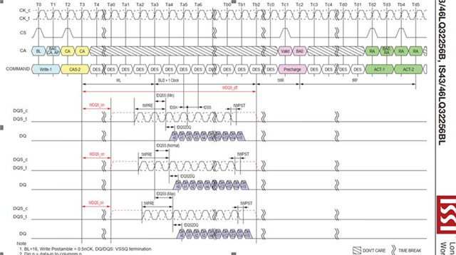
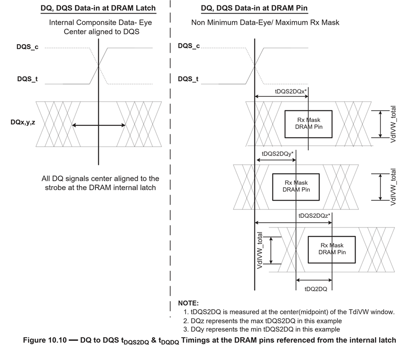
Figure 1 shows the timing of LPDDR4 write operations
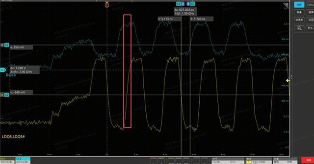
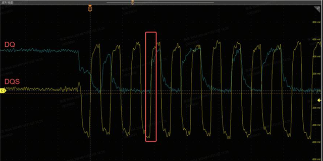
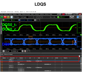
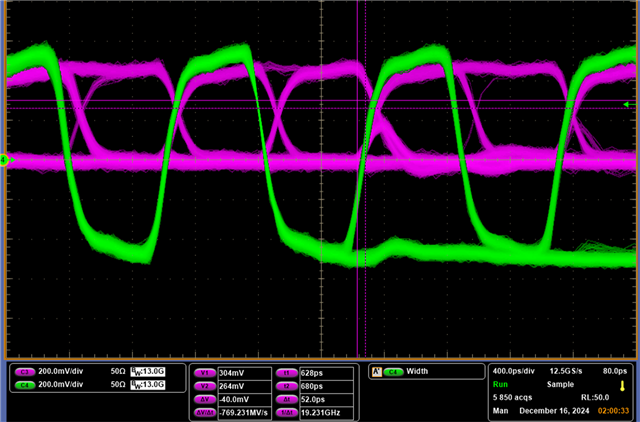
Figure 2 shows the waveform we tested
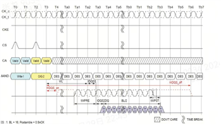
Figure 1 shows the timing of LPDDR4 write operations
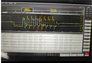
Figure 2 shows the waveform we tested