Part Number: MSP432E401Y
Tool/software:
Hi TI,
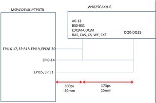
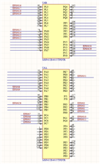
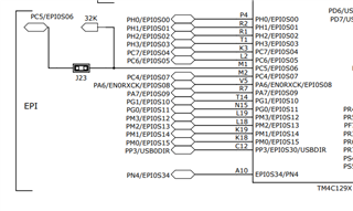
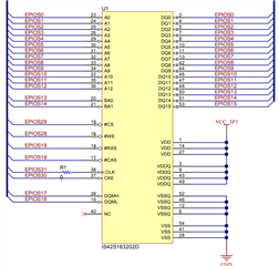
I need to connect an SDRAM memory to the MSP432E401Y through the EPI interface,
1-) Can I use the W9825G6KH-6 memory? Is it compatible with the EPI interface?
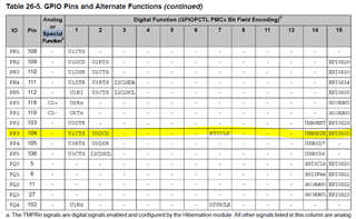
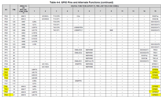
2-) I attach the connection diagram between the SDRAM memory and the MSP432E401Y. Is the attached schematic correct? Note EPI0S0-12 is shared between address bus and data bus, while EPI0S13-14 is shared between data bus and bank select. Is this correct?
3-) Does the schematic require additional components such as termination resistors or something else (I am referring only to the part related to the memory)?
Thanks very much. Best regards.