This thread has been locked.

If you have a related question, please click the "Ask a related question" button in the top right corner. The newly created question will be automatically linked to this question.

TM4C123BH6ZRB: TM4C123BH6ZRBI7

Part Number: TM4C123BH6ZRB
Other Parts Discussed in Thread: INA240, CDCV304

Tool/software:

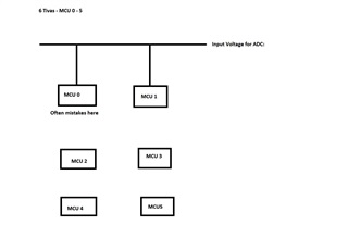
In a two-channel system A and B, with three TM4C123BH6 (BGA 157) per channel measure analog signals.

Measuring current of max. 3A, it is an accuracy of 0.1% deviation between the channels and against an external measurement required.

We have a problem with the ADC inputs. For example A0_I on MCU0 (PD5) measures 3 to 5 digits wrong. All other ADC imputs on this MCU have the same behaviour. 

It's sporadically, tempereture has no impact and when the failure occures it is constant till the next restart.

The test software is as minimal as possible. The ADC and two GPIOs with LEDs there are configured.


The electrical design is not perfect, but the placement is almost identical, only the routing is different.

  • Instead of the max. 4µF at the digital supply VDD, a single X7R 4.7µF capacitor (C455) is installed.
  • VREFA+ is supplied by an external reference source with 3.3V and 0.1% tolerance via a ferrite bead and the recommended block capacitors.
  • A voltage from a current generated by an INA240 is applied to the ADC input via a pull-down of 10k Ohm (R472), which is fed through a low-pass filter with 10k Ohm (R504) and 100nF (C472).
    According to application note SPNA061, Cext should have approx. 40 nF (C106) and Rsource 410 Ohm (R504).

Chances in the component values doesn’t show any improvement.


For measurement purposes, the INA240 was disconnected and a external voltage source with low ripple was applied. This also shows a difference between the channels.

If the ADC input is open, there can be measured some 10 millivolts that are higher to other MCUs and ADC inputs.


Could this be crosstalk?

  • We have a problem with the ADC inputs. For example A0_I on MCU0 (PD5) measures 3 to 5 digits wrong. All other ADC imputs on this MCU have the same behaviour. 

    3 to 5 LSB of error is a lot.

    Can you run the your custom software on the LaunchPad and what is the result?

    Can you run the stock TivaWare example on your custom board and what is the result?

    You said A0_1. Is this AIN0 you are referring to? If you meant AIN0 then it is on PE3, not PD6. PD5 is for AIN6. Please clarify. 

    What is your clock source to the ADC? There are several known ADC errata and see if they apply to you. Please also go through errata sheet at https://www.ti.com/lit/pdf/spmz849 for details. 

  •  aksed:
    You said A0_1. Is this AIN0 you are referring to? If you meant AIN0 then it is on PE3, not PD6. PD5 is for AIN6. Please clarify. 

    Sorry. Our internal naming is A0_MCU0_i and is connected to PD5. AIN0 is connected to A3_MCU0_U.

  • HI,

     Thanks for the clarification. Can you also answer the other questions I raised earlier?

      Please note that today is a public holiday for TI. Please expect delay in my response. 

  • Hello Charles,

    the software runs on the launchpad without any problems.

    The sample code on our board also causes this error.

    The code we use doesn't differ much from the example code. This can be seen below:


    /* ISR Adc0 - Sequence 0 */
    void Adc_IsrTestChASeq0()
    {
    uint32_t AdcQueue[8];

    ADCIntClear( ADC0_BASE, 0);

    ADCSequenceDataGet( ADC0_BASE, 0, AdcQueue);

    /* We apply a 5 mV voltage to the ADC (PD5). If voltage below or equal 3 LSB => Red LED on else OFF */
    if(AdcQueue[0] <=3)
    {
    // LED_ON
    GPIOPinWrite( GPIO_PORTG_AHB_BASE, PINS_MCU0_LED1, GPIO_PIN_6); // PG6
    }
    else
    {
    // LED_OFF
    GPIOPinWrite( GPIO_PORTG_AHB_BASE, PINS_MCU0_LED1, ~GPIO_PIN_6); //PG6
    }
    }


    int main(void)
    {
    SysCtlClockSet(SYSCTL_SYSDIV_2_5 | SYSCTL_USE_PLL | SYSCTL_XTAL_8MHZ | SYSCTL_OSC_MAIN);
    SysCtlDelay( DEV_EN_DELAY);

    SysCtlGPIOAHBEnable(SYSCTL_PERIPH_GPIOB);
    SysCtlPeripheralEnable(SYSCTL_PERIPH_GPIOB);

    SysCtlGPIOAHBEnable( SYSCTL_PERIPH_GPIOD);
    SysCtlPeripheralEnable( SYSCTL_PERIPH_GPIOD);

    SysCtlGPIOAHBEnable( SYSCTL_PERIPH_GPIOG);
    SysCtlPeripheralEnable( SYSCTL_PERIPH_GPIOG);

    SysCtlPeripheralEnable( SYSCTL_PERIPH_GPIOM);

    /* enable Adc */
    SysCtlPeripheralEnable( SYSCTL_PERIPH_ADC0);
    while(!SysCtlPeripheralReady(SYSCTL_PERIPH_ADC0));

    /* enable timer for adc-measurement*/
    SysCtlPeripheralEnable( SYSCTL_PERIPH_TIMER1);
    while(!SysCtlPeripheralReady(SYSCTL_PERIPH_TIMER1));

    /* configure LED (PG6) for debugging*/
    GPIOPinTypeGPIOOutput( GPIO_PORTG_AHB_BASE, GPIO_PIN_6 );
    GPIOPadConfigSet( GPIO_PORTG_AHB_BASE, GPIO_PIN_6, 0, GPIO_PIN_TYPE_STD);

    // configure PD5 - A0
    GPIOPinTypeADC( GPIO_PORTD_AHB_BASE, PINS_A0_MCU0_I );
    GPIOPadConfigSet( GPIO_PORTD_AHB_BASE, PINS_A0_MCU0_I, 0, GPIO_PIN_TYPE_ANALOG);


    /* init ADC */
    ADCReferenceSet(ADC0_BASE, ADC_REF_EXT_3V);

    ADCSequenceDisable(ADC0_BASE, 0);

    /* adc trigger by timer */
    ADCSequenceConfigure( ADC0_BASE, 0, ADC_TRIGGER_TIMER, 0);

    /* PD5 */
    ADCSequenceStepConfigure( ADC0_BASE, 0, 0, ADC_CTL_CH6 | ADC_CTL_IE | ADC_CTL_END);

    ADCSequenceEnable( ADC0_BASE, 0);

    /* isr */
    ADCIntRegister( ADC0_BASE, 0, Adc_IsrTestChASeq0);

    ADCIntClear( ADC0_BASE, 0);
    ADCIntEnable( ADC0_BASE, 0);
    IntPrioritySet(INT_ADC0SS0, 0x00);
    IntEnable((uint32_t)INT_ADC0SS0);


    /* configure timer for adc measurement */
    TimerConfigure( TIMER1_BASE, TIMER_CFG_PERIODIC);

    // Set timer clock source to system clock (80Mhz)
    TimerClockSourceSet( TIMER1_BASE, TIMER_CLOCK_SYSTEM);

    IntPrioritySet(INT_TIMER1A, 0x00);

    // should result in 80M/8000Hz = 10000 (125µs)
    TimerLoadSet( TIMER1_BASE, TIMER_A, 10000);

    // make the timer trigger an adc conversion
    TimerADCEventSet( TIMER1_BASE, TIMER_ADC_TIMEOUT_A);
    TimerControlTrigger( TIMER1_BASE, TIMER_A, true);

    // enable timer
    TimerEnable( TIMER1_BASE, TIMER_A );


    while(1) {}
    }

  • /* We apply a 5 mV voltage to the ADC (PD5). If voltage below or equal 3 LSB => Red LED on else OFF */
    if(AdcQueue[0] <=3)

    Hi,

     First of all, 5mV is equal to about 6 (000000000110) as in 0.005/3.3*4096. What do you actually read? I'm not sure why you are comparing with a value of 3 (000000000011). A value of 3 does not mean 3 LSB. A 3 LSB variation means the sample value is off by up to 2^3=8. In another word, for an expected sampled value of 6 you are reading 6+8=14 to have a 3LSB error. 

    Do you have the VDDA connected to a table supply if you are using it? I see that you use ADC_REF_EXT_3V. 

    The sample code on our board also causes this error.

    Which sample code did you use?

    Why don't you try the stock example and only change from AIN0 to AIN6. What sample value do you read? Below is the stock example. You might need to also change the clock setting since you are using a 8Mhz crystal on your custom board. Perhaps you can try using the internal PIOSC as the clock source for System clock. 

    #include <stdbool.h>
    #include <stdint.h>
    #include "inc/hw_memmap.h"
    #include "driverlib/adc.h"
    #include "driverlib/gpio.h"
    #include "driverlib/pin_map.h"
    #include "driverlib/sysctl.h"
    #include "driverlib/uart.h"
    #include "utils/uartstdio.h"
    
    //*****************************************************************************
    //
    //! \addtogroup adc_examples_list
    //! <h1>Single Ended ADC (single_ended)</h1>
    //!
    //! This example shows how to setup ADC0 as a single ended input and take a
    //! single sample on AIN0/PE3.
    //!
    //! This example uses the following peripherals and I/O signals.  You must
    //! review these and change as needed for your own board:
    //! - ADC0 peripheral
    //! - GPIO Port E peripheral (for AIN0 pin)
    //! - AIN0 - PE3
    //!
    //! The following UART signals are configured only for displaying console
    //! messages for this example.  These are not required for operation of the
    //! ADC.
    //! - UART0 peripheral
    //! - GPIO Port A peripheral (for UART0 pins)
    //! - UART0RX - PA0
    //! - UART0TX - PA1
    //!
    //! This example uses the following interrupt handlers.  To use this example
    //! in your own application you must add these interrupt handlers to your
    //! vector table.
    //! - None.
    //
    //*****************************************************************************
    
    //*****************************************************************************
    //
    // This function sets up UART0 to be used for a console to display information
    // as the example is running.
    //
    //*****************************************************************************
    void
    InitConsole(void)
    {
        //
        // Enable GPIO port A which is used for UART0 pins.
        // TODO: change this to whichever GPIO port you are using.
        //
        SysCtlPeripheralEnable(SYSCTL_PERIPH_GPIOA);
    
        //
        // Configure the pin muxing for UART0 functions on port A0 and A1.
        // This step is not necessary if your part does not support pin muxing.
        // TODO: change this to select the port/pin you are using.
        //
        GPIOPinConfigure(GPIO_PA0_U0RX);
        GPIOPinConfigure(GPIO_PA1_U0TX);
    
        //
        // Enable UART0 so that we can configure the clock.
        //
        SysCtlPeripheralEnable(SYSCTL_PERIPH_UART0);
    
        //
        // Use the internal 16MHz oscillator as the UART clock source.
        //
        UARTClockSourceSet(UART0_BASE, UART_CLOCK_PIOSC);
    
        //
        // Select the alternate (UART) function for these pins.
        // TODO: change this to select the port/pin you are using.
        //
        GPIOPinTypeUART(GPIO_PORTA_BASE, GPIO_PIN_0 | GPIO_PIN_1);
    
        //
        // Initialize the UART for console I/O.
        //
        UARTStdioConfig(0, 115200, 16000000);
    }
    
    //*****************************************************************************
    //
    // Configure ADC0 for a single-ended input and a single sample.  Once the
    // sample is ready, an interrupt flag will be set.  Using a polling method,
    // the data will be read then displayed on the console via UART0.
    //
    //*****************************************************************************
    int
    main(void)
    {
    #if defined(TARGET_IS_TM4C129_RA0) ||                                         \
        defined(TARGET_IS_TM4C129_RA1) ||                                         \
        defined(TARGET_IS_TM4C129_RA2)
        uint32_t ui32SysClock;
    #endif
    
        //
        // This array is used for storing the data read from the ADC FIFO. It
        // must be as large as the FIFO for the sequencer in use.  This example
        // uses sequence 3 which has a FIFO depth of 1.  If another sequence
        // was used with a deeper FIFO, then the array size must be changed.
        //
        uint32_t pui32ADC0Value[1];
    
        //
        // Set the clocking to run at 20 MHz (200 MHz / 10) using the PLL.  When
        // using the ADC, you must either use the PLL or supply a 16 MHz clock
        // source.
        // TODO: The SYSCTL_XTAL_ value must be changed to match the value of the
        // crystal on your board.
        //
    #if defined(TARGET_IS_TM4C129_RA0) ||                                         \
        defined(TARGET_IS_TM4C129_RA1) ||                                         \
        defined(TARGET_IS_TM4C129_RA2)
        //
        // Note: SYSCTL_CFG_VCO_240 is a new setting provided in TivaWare 2.2.x and
        // later to better reflect the actual VCO speed due to SYSCTL#22.
        //
        ui32SysClock = SysCtlClockFreqSet((SYSCTL_XTAL_25MHZ |
                                           SYSCTL_OSC_MAIN |
                                           SYSCTL_USE_PLL |
                                           SYSCTL_CFG_VCO_240), 20000000);
    #else
        SysCtlClockSet(SYSCTL_SYSDIV_10 | SYSCTL_USE_PLL | SYSCTL_OSC_MAIN |
                       SYSCTL_XTAL_16MHZ);
    #endif
    
        //
        // Set up the serial console to use for displaying messages.  This is
        // just for this example program and is not needed for ADC operation.
        //
        InitConsole();
    
        //
        // Display the setup on the console.
        //
        UARTprintf("ADC ->\n");
        UARTprintf("  Type: Single Ended\n");
        UARTprintf("  Samples: One\n");
        UARTprintf("  Update Rate: 250ms\n");
        UARTprintf("  Input Pin: AIN0/PE3\n\n");
    
        //
        // The ADC0 peripheral must be enabled for use.
        //
        SysCtlPeripheralEnable(SYSCTL_PERIPH_ADC0);
    
        //
        // For this example ADC0 is used with AIN0 on port E7.
        // The actual port and pins used may be different on your part, consult
        // the data sheet for more information.  GPIO port E needs to be enabled
        // so these pins can be used.
        // TODO: change this to whichever GPIO port you are using.
        //
        SysCtlPeripheralEnable(SYSCTL_PERIPH_GPIOE);
    
        //
        // Select the analog ADC function for these pins.
        // Consult the data sheet to see which functions are allocated per pin.
        // TODO: change this to select the port/pin you are using.
        //
        GPIOPinTypeADC(GPIO_PORTE_BASE, GPIO_PIN_3);
    
        //
        // Enable sample sequence 3 with a processor signal trigger.  Sequence 3
        // will do a single sample when the processor sends a signal to start the
        // conversion.  Each ADC module has 4 programmable sequences, sequence 0
        // to sequence 3.  This example is arbitrarily using sequence 3.
        //
        ADCSequenceConfigure(ADC0_BASE, 3, ADC_TRIGGER_PROCESSOR, 0);
    
        //
        // Configure step 0 on sequence 3.  Sample channel 0 (ADC_CTL_CH0) in
        // single-ended mode (default) and configure the interrupt flag
        // (ADC_CTL_IE) to be set when the sample is done.  Tell the ADC logic
        // that this is the last conversion on sequence 3 (ADC_CTL_END).  Sequence
        // 3 has only one programmable step.  Sequence 1 and 2 have 4 steps, and
        // sequence 0 has 8 programmable steps.  Since we are only doing a single
        // conversion using sequence 3 we will only configure step 0.  For more
        // information on the ADC sequences and steps, reference the datasheet.
        //
        ADCSequenceStepConfigure(ADC0_BASE, 3, 0, ADC_CTL_CH0 | ADC_CTL_IE |
                                 ADC_CTL_END);
    
        //
        // Since sample sequence 3 is now configured, it must be enabled.
        //
        ADCSequenceEnable(ADC0_BASE, 3);
    
        //
        // Clear the interrupt status flag.  This is done to make sure the
        // interrupt flag is cleared before we sample.
        //
        ADCIntClear(ADC0_BASE, 3);
    
        //
        // Sample AIN0 forever.  Display the value on the console.
        //
        while(1)
        {
            //
            // Trigger the ADC conversion.
            //
            ADCProcessorTrigger(ADC0_BASE, 3);
    
            //
            // Wait for conversion to be completed.
            //
            while(!ADCIntStatus(ADC0_BASE, 3, false))
            {
            }
    
            //
            // Clear the ADC interrupt flag.
            //
            ADCIntClear(ADC0_BASE, 3);
    
            //
            // Read ADC Value.
            //
            ADCSequenceDataGet(ADC0_BASE, 3, pui32ADC0Value);
    
            //
            // Display the AIN0 (PE3) digital value on the console.
            //
            UARTprintf("AIN0 = %4d\r", pui32ADC0Value[0]);
    
            //
            // This function provides a means of generating a constant length
            // delay.  The function delay (in cycles) = 3 * parameter.  Delay
            // 250ms arbitrarily.
            //
    #if defined(TARGET_IS_TM4C129_RA0) ||                                         \
        defined(TARGET_IS_TM4C129_RA1) ||                                         \
        defined(TARGET_IS_TM4C129_RA2)
            SysCtlDelay(ui32SysClock / 12);
    #else
            SysCtlDelay(SysCtlClockGet() / 12);
    #endif
        }
    }

  • The code was just simplified and an LED was used to visually indicate the error. 
    At the beginning of our investigation, we evaluated the ADC raw value ((adc_rawValue / 4096) * 3.3) and had it displayed.
    Then we noticed that we can also see the error if we apply a stable 5mV and turn on the red LED if the raw value is less 
    than or equal to 3.

    As a reminder, we have 6 Tivas on our board and they all behave differently. But the software is the same for everyone! 
    Each controller simply boots up and measures ADC_CTL_CH6 every 125µs. If the ADC raw value is less than or equal to 3, 
    the LED turns on. We get one of the 6 controllers in a state where the LED permanently shows the error, i.e. permanently falls below an ADC
    raw value of 4. When we had the measurements displayed earlier, we found that at a stable 5mV the ADC displayed values ​​between 0 and 3 mV.
    With the LED we can now see that it stays on for one controller and is off for all others (so they measure the 5mV correctly).
    So only one controller seems to have this problem. And with all of its ADC inputs! The error can be provoked with all AIN's.
    And very importantly, the problem only occurs sporadically. When restarting the board. But even if you restart the Tiva with 
    SysCtlReset()...
    If you restart the controller again and again, it can happen at some point that the error occurs (LED on) and remains permanent
    until you restart again. But only on one of the 6 tivas with identical software! We have already tried to apply an absolutely stable external reference voltage to the ADC and use an oscilloscope to make sure
    that it is stable. We apply an absolutely stable 5mV to the adc. So far no success. We would also like to try using the internal PIOSC as a system clock. We are grateful for every tip, because we are slowly running
    out of ideas. Precisely because out of 6 (mcu0 - mcu5) tivas on the board, it always reliably affects the first one (mcu0).
    And this applies to every board that we examined.

    In my opinion this is a hardware problem, but we had to fix it.
    The question is what can bother the ADC so much that it permanently has this problem, and what can be done about it.
  • We get one of the 6 controllers in a state where the LED permanently shows the error, i.e. permanently falls below an ADC
    raw value of 4.
    So only one controller seems to have this problem. And with all of its ADC inputs! The error can be provoked with all AIN's.

    Hi Benjamin,

      Thanks for the additional information. Earlier I was under the impression that all six are producing vastly different results (up to 5 LSBs of difference). It looks like there is only one to focus on. While I don't know why this particular chip behaves worst than the other five, I think it is within the spec. Please find the ADC electrical characteristic.  

    We get one of the 6 controllers in a state where the LED permanently shows the error, i.e. permanently falls below an ADC
    raw value of 4. When we had the measurements displayed earlier, we found that at a stable 5mV the ADC displayed values ​​between 0 and 3 mV.

    One step is equal to 3.3/4096 = 0.806mV. If you measure 3mV for an 5mV input then the error is (5-3)/0.806=2.48LSB. But if you are measuring 0V with an 5mV input then it is 5/0.806=6.2LSB and I agree this is over the spec. 

    And very importantly, the problem only occurs sporadically. When restarting the board. But even if you restart the Tiva with
    SysCtlReset()...
    If you restart the controller again and again, it can happen at some point that the error occurs (LED on) and remains permanent
    until you restart again. But only on one of the 6 tivas with identical software!

    I'm interested to know if the errors you are seeing is only for low voltages on AIN or you see the same with other input voltages such as 1.65V or 3.3V? 

     I do want to point out that for low voltage input, the amount of nonlinearity error will be usually higher. The below link has some discussion about it. 

    https://electronics.stackexchange.com/questions/226931/adc-error-for-low-voltage-measurements

    We have already tried to apply an absolutely stable external reference voltage to the ADC and use an oscilloscope to make sure
    that it is stable. We apply an absolutely stable 5mV to the adc. So far no success.

    ok. Understand that it is not due to unstable VDDA or GNDA. 

    The question is what can bother the ADC so much that it permanently has this problem, and what can be done about it.

    Normally for best ADC performance the below options are recommended but I believe you have done some of them already. Again, please bear in mind the intrinsic linearity error as specified in the datasheet. 

    • Use external Vref
    • Have separate VDDA and GNDA from VDD and GND
    • Adding RC filter.
    • Short trace of the input signal
    • Add a unity gain buffer driver
    • Oversampling/Averaging of the input. TM4C123 has a hardware sample averaging circuit
  • Understand that it is not due to unstable VDDA or GNDA

    • Use external Vref ⇒ We use a reference with 3.3 V, 0.1% tolerance and 10 mA output current for three controllers.
    • Have separate VDDA and GNDA from VDD and GND  No, there is one plane for GND
    • Adding RC filter. ⇒ Yes, the AINs have a low pass filter with cut off frequency at 160 Hz
    • Short trace of the input signal ⇒ not possible
    • Add a unity gain buffer driver ⇒ not included, the design is freezed

    There is a spike in VREF+ (L3-1) measured with a differential probe to C10-2. After removing L3 VREF+ is clean, but the error is still present.

    Also done with L2, but same effect.

    gn: VREF+, or: AIN

    gn: VREF+, or: AIN

    L3 removed

    gn: VREF+, or: AIN

    I'm interested to know if the errors you are seeing is only for low voltages on AIN or you see the same with other input voltages such as 1.65V or 3.3V? 

    Yes, we checked it with other input voltages, with same behaviour.

  • Yes, we checked it with other input voltages, with same behaviour.

    Hi,

      Can you show me the raw data that you measure at 0V, 5mV, 1.65V and 3.3V for the problem board vs. the good boards?

      Can you do a ABA swap test by swapping the suspected MCU to one of the other five boards that you said have no issues? Please do the same by swapping the MCU on one of the five working boards to the suspected board. 

     Although not likely to explain the problem, can you show Lot Trace Code on the six chips?

  • Hi Charles,

    it seems like we haven't explained something quite right yet. 
    It's about multiple boards, that's right. There are 6 Tivas on each board. 
    Always one Tiva (the same in terms of position) reliably has the error.
    For the others, the error occurs much less frequently or not at all.


    The error only occurs when the board is completely restarted or when the Tiva is SysCtlReset().
    We've also tried resetting just the ADC peripherals, but that has no effect.

    I will carry out the measurements again later, then I will write the desired ADC raw values ​​here.
     
  • it seems like we haven't explained something quite right yet. It's about multiple boards, that's right. There are 6 Tivas on each board.
    Always one Tiva (the same in terms of position) reliably has the error.
    For the others, the error occurs much less frequently or not at all.


    Hi Benjamin,

      Sorry for my past misunderstanding. You are saying each board has six Tiva and you have multiple of such board. It is always the MCU0 that is giving an undesirable ADC measurement no matter which board you use. The MCU1,2,3,4,5 are mostly correct on the boards. Is that a correct understanding? If that is the case, something is peculiar on the physical position of MCU0 vs other Tiva MCUs on the boards. 

  • Hi Charles,

    Yes, the hardware is slightly different. 
    The strange thing is that the error then occurs permanently.
    But it's enough to restart the tiva with SysCtlReset() and the error is gone.
    More precisely, the "raffle" starts again - it may be that the error occurs
    again immediately or only after several restarts of the Tiva.
  • Hi Benjamin,

      Can you do a ABA swap between the MCU0 and MCU5? I'm curious to know if MCU5 will suddenly exhibit the same issue like MCU0 while MCU0 becomes normal once moved to the MCU5 position. 

      Since your hardware is frozen, we need to see if any software approach may improve the ADC result. Can you try:

      - Slow down the sample rate by writing to the ADCPC register? By default, it is 1Msps. Try 500ksps or lower. Does it make a difference?


      - Enable Dithering.

      - Can you try ADC1 instead of ADC0? does it give the same issue?

    - Can you try the hardware averaging?

    - Can you try with internal Vref instead of external Vreg. I'm curious to know if that makes a difference?

    The strange thing is that the error then occurs permanently.

    I'm still not clear with this observation. You seem to suggest the errors become accumulative over time. 

  • What I mean by this is that if the error occurs due to restarts, then the "offset" basically remains.

    We have already tried out a lot of what you write here.

    Used the ADC 1 instead of 0, used dithering, used hardware average, used the internal VREF, and also changed the sample rate.

    Nothing has been successful so far.

    In my tests I could now see that the MCU0 is drifting downwards and the MCU1 is drifting upwards.

    It happens much more often in the MCU0, which is why the MCU1 hasn't been noticed until now. 

    I also noticed that the MCU0 doesn't drift up, only down, and the MCU1 that it drifts down, not up (I stopped the tests after about 1000 restarts)

    So far, 3 of the boards tested have this behavior.

    **************************************************************************************

    By drifting (or offset) I mean when I use the test setup as an example for the MCU0:
    -stable 5mA on the adc
    -restart until the raw ADC value falls below 4
    - once below 4 then no more restarts.

    I get this behavior from now on:
    -Without another restart, the ADC raw values ​​of less than 4 now accumulate

    (there are still values ​​of 5,6,7 - but more often less than 4).

    ***************************************************************************************

  • Hi Benjamin,

    We have already tried out a lot of what you write here.

    Used the ADC 1 instead of 0, used dithering, used hardware average, used the internal VREF, and also changed the sample rate.

    Nothing has been successful so far.

    ok.

    In my tests I could now see that the MCU0 is drifting downwards and the MCU1 is drifting upwards.

    It happens much more often in the MCU0, which is why the MCU1 hasn't been noticed until now. 

    I also noticed that the MCU0 doesn't drift up, only down, and the MCU1 that it drifts down, not up (I stopped the tests after about 1000 restarts)

    So far, 3 of the boards tested have this behavior.

    So far you have provided the raw data for a 5mV input. As I have requested before, I'm curious to know the raw data at other points (e.g. 0V, 1.65V, 3.3V). Can you provide them?

    By drifting (or offset) I mean when I use the test setup as an example for the MCU0:
    -stable 5mA on the adc
    -restart until the raw ADC value falls below 4
    - once below 4 then no more restarts.

    I get this behavior from now on:
    -Without another restart, the ADC raw values ​​of less than 4 now accumulate

    (there are still values ​​of 5,6,7 - but more often less than 4).

    Now I understand your setup as to what you mean by the error becomes permanent. 

    Have you had a chance to do the ABA swap between MCU0 and MCU5?

    What clock source do you provide to the ADC? Can you try to use MOSC as the clock source for ADC?

    I have looked at your schematic for VDDA and VREF+ and it is in compliance with the recommendation from TM4C129 System Design Guideline. As far as the layout goes, you only show for one of them. I suppose the layout is pretty much the same for all six MCUs on the board, correct?

    Do you have a blower that you can blow on top of the MCU under test? I'm curious to know if temperature plays a role here as the temperature rises up over time. You said that perhaps after 1000 restarts the error becomes permanent. I hope with a blower, it will provide a better heat dissipation. Does it improve? It will be good if you can also record the temperature at start and at the point when the error becomes permanent with and without the blower. 

  • Contribution from Benjamin:

    Sorry, yes we tried it with 3.3V stable input on the ADC. The error detection is then set on MCU0 when the ADC raw value falls below 4093. 
    and it happens here too. The behavior is the same as with the stable 5mV. That's why I always talk about it.

    Yesterday we used the internal clock. Here the values initially fluctuated more. That's why we used dithering and hardware oversample (4). 
    We haven't been able to see the error anymore (at least that's how it seems after many attempts). 
    When we then used the external clock again with the same configuration, the error was there again.

  • Sorry, yes we tried it with 3.3V stable input on the ADC. The error detection is then set on MCU0 when the ADC raw value falls below 4093. 
    and it happens here too. The behavior is the same as with the stable 5mV. That's why I always talk about it.

    Hi Markus/Benjamin,

      Ok. I suppose for 1.65V, you have the same error, correct?

    Yesterday we used the internal clock. Here the values initially fluctuated more. That's why we used dithering and hardware oversample (4). 
    We haven't been able to see the error anymore (at least that's how it seems after many attempts). 
    When we then used the external clock again with the same configuration, the error was there again.

    Glad that you are seeing some improvements.

    You are saying with the internal clock, dithering and hardware oversample the error somehow went away. Is that correct? Can you run overnight and see if the problem truly went away?

    I suppose you use the ADCClockConfigSet() to configure PIOSC as the clock source for ADC. Is that correct? Is the below how you call the API? If not, can you provide the exact API call you use?

    ADCClockConfigSet(ADC0_BASE, ADC_CLOCK_SRC_PIOSC | ADC_CLOCK_RATE_FULL, 1);

    What was the clock you used before? 

    Did you have a chance to do a swap between MCU0 and MCU5 as I'm very keen to know if the physical location of the MCU on the board plays a role here. 

    Did you have a chance to blow air over the MCU under test? Does it make a difference?

  • Heat is not the problem.

    The physical locations is fix and a swap can't execute.

    In the design is for clocking the MCUs the clock buffer CDCV304 with an oscillator of 8 MHz. The clock buffer has no blocking capacitor and so there are spikes on the voltage supply.

    On the trace from the clock buffer via a resistor of 33 Ohm to the MCU OSC0 input there are reflections and glitches.

    From high to low the signal falls two times below VIL as specified the the datasheet chapter 23.9.5. 

    There is a hint in the datasheet regarding ADC operation "a. Clock frequency (plus jitter) must be stable..."

    Can this lead to a problem?

  • In the design is for clocking the MCUs the clock buffer CDCV304 with an oscillator of 8 MHz. The clock buffer has no blocking capacitor and so there are spikes on the voltage supply.

    Do you have the PLL enabled?

    Can you cut the trace to OSCIN and supply a clean 16Mhz clock using a function generator to MCU0? Will you see any difference? Earlier you said if you use the internal clock source (PIOSC at 16Mhz) then the problem seems to go away. Is that still the case?

  • Hi,

      I have not heard back from you.  I will close the thread for now. If you have any update, you can write back to this post and the status will change to OPEN.