This thread has been locked.

If you have a related question, please click the "Ask a related question" button in the top right corner. The newly created question will be automatically linked to this question.

MSPM0G1507: BCR configuration to disable SWD and BSL configuration to configure uart baudrate

Part Number: MSPM0G1507
Other Parts Discussed in Thread: MSPM0G3507, , UNIFLASH, SYSCONFIG

Tool/software:

Hi TI Expert,

I am working on a project based on uart_echo_LP_MSPM0G3507_freertos_ticlang, but I have changed the target device to MSPM0G1507 and updated the linker command file to mspm0g1507.cmd.

Project Details:

  • Device: MSPM0G1507
  • SDK Version: 2.1.0.03

Objectives:

  1. Change the BSL UART baud rate to 115200 (using pins PA10 and PA11).
  2. Disable SWD in production while ensuring the BSL update function remains available.

My Current Understanding of BSL:

  1. My project (using the default mspm0g1507.cmd) can already be updated using the BSL_GUI_EXE tool.
  2. The internal boot ROM runs first and utilizes BCR and BSL config settings, which can be configured. It may also reference the .vtable, though I am uncertain.
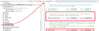
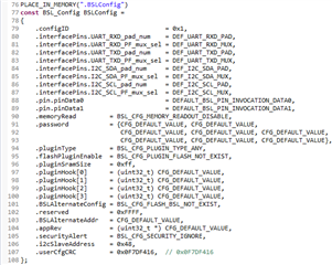
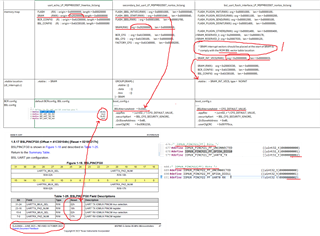
  3. BSL-related example projects contain boot_config.c, which defines BCR and BSL configurations, and each project has different memory layouts in the linker file. check the figure attached
  4. BCR configuration has an option to enable or disable SWD.
  5. The internal boot ROM determines whether to execute the built-in BSL or use a BSL plugin.
  6. The BSL plugin has an Init function, which can be used to configure the UART baud rate.
  7. The BSL configuration allows specifying a secondary bootloader, which can bypass the built-in BSL.

Questions:

  1. Does the boot ROM run completely independently by default? If not, does it rely on .vtable? If it does, how does it access the vector table, considering different projects place .vtable at different locations?
  2. Why do different projects have different SRAM start addresses (0x20200000 vs. 0x20000000)? What determines this?
  3. To change the BSL UART baud rate, do I need to use the plugin Init function? If so, do I also need to provide the Send, Receive, and Deinit functions?
  4. How should I modify my linker command file (.cmd) to incorporate the above requirements?

I would greatly appreciate your insights on these questions.

Best regards,

  • Hi Zhuang, 
    Let me consult with our team regarding your two first questions. As for the last two, I would recommend looking into the bsl_software_invoke_app_demo_uart_LP_MSPM0G3507_nortos_ticlang example we have in our SDK for more reference.
    Best Regards,
    Diego Abad

  • Hi Diego,

    Thanks for your response.

    After reviewing the example, my understanding is that it demonstrates how an application can proactively put the chip into BSL mode (e.g., by receiving 0x22 over UART or detecting a button press).

    However, my main question is: How can I change the default BSL baud rate from 9600 to 115200?

    • To achieve this, I believe modifications are needed in the linker file, BCR configuration, and BSL settings.
    • Could you confirm if this approach is correct and guide me on the necessary changes?

    Thanks in advance!

  • Hi Zhuang,
    My understanding is that the UART BSL pins can be changed the baud rate through initializing the module. However, let me confirm with my team about this on Monday.

    Best Regards,

    Diego Abad

  • Hi Zhuang,
    1. ROM runs after BOOTRST. This behavior you can assume to be independent from any configuration to the device.

    2. This is determined by the project's settings. The 0x2020 is the unprotected part of SRAM while 0x2000 is the default part of SRAM.

    For the last two questions, you can change the baud rate through a Change Baud Rate command. For more information I'm attaching the MSPM0 Bootloader User's Guide and the MSPM0 Bootloader (BSL) Implementation (Rev. C)

    Best Regards,

    Diego Abad

  • Hi Diego,

    Thanks for your response.

    I still have a few remaining questions that I’d like to clarify. Could you help explain them further?

    1. For 1. I’m still confused about why the linker file in the BSL_interface project mentions that the vector table must comply with the internal BSL vector table. Could you clarify this?

    2. Could you explain why standard MSPM0G3507 projects have their SRAM starting at 0x20200000, while BSL-related projects use 0x20000000?

      • What is the actual physical SRAM address for MSPM0G1507 and MSPM0G3507?
      • How does this difference impact memory allocation?

    I very appreciate your insights!

  • Hi Zhuang,
    1. This is just a requirement you need to follow. It's a design choice.
    2. The reason is that BSL always requires the use of the 0x2000 address in SRAM (after clearing that section). If not used in this region, BSL won't work as intended. The actual physical address is SRAM for both G devices is in  Table 1-2. SRAM Region Memory Map in the Userguide. The difference between one address and the other is the type of integrity checks applied to the access.
    Best Regards,
    Diego Abad

  • Hi Diego,

    I am trying to change the BSL password in my project. After modifying it and recalculating the new CRC, I am unable to successfully flash the firmware.

    To troubleshoot, I attempted flashing the BCR and BSL sections with default values, which match the factory constants. However, when flashing the .txt file using UniFlash (with "Erase MAIN and NONMAIN memory" checked), the process still fails.

    I have attached a screenshot for reference.

    Could you guide me on how to properly integrate the BCR and BSL sections into my project and correctly change the BSL password?

    Additional Information:

    • I am using a uart_echo_LP_MSPM0G3507_freertos_ticlang example project that does not include SysConfig.

    Looking forward to your advice.

  • Hi Zhuang,
    I will recommend posting this question as a different E2E thread. 
    Best Regards,
    Diego Abad