This thread has been locked.

If you have a related question, please click the "Ask a related question" button in the top right corner. The newly created question will be automatically linked to this question.

TM4C1294NCPDT: TM4C1294NCPDT

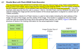
Part Number: TM4C1294NCPDT

Tool/software:

I Have requirement to load the hex file into RAM for firmware upgrade and boot from RAM , can you please help me to do the changes in Linker file to
use the RAM for both vtable section for Bootloader Application and to write the hex file for Firmware upgrade HEX file and boot from there 

When I try to write in RAM section beyond the memory region allocated for execution Its is writing only "0" zeros.

Can you Please suggest how to partition the RAM for  Application Vtable section and to write firmware upgrade Hex file  via Ethernet.

can you also please review the linker file for any changes to be made
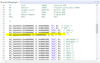
/******************************************************************************
 * Copyright (c) 2013-2017 Texas Instruments Incorporated.  All rights reserved.
 * Software License Agreement
 * 
 * Texas Instruments (TI) is supplying this software for use solely and
 * exclusively on TI's microcontroller products. The software is owned by
 * TI and/or its suppliers, and is protected under applicable copyright
 * laws. You may not combine this software with "viral" open-source
 * software in order to form a larger program.
 * 
 * THIS SOFTWARE IS PROVIDED "AS IS" AND WITH ALL FAULTS.
 * NO WARRANTIES, WHETHER EXPRESS, IMPLIED OR STATUTORY, INCLUDING, BUT
 * NOT LIMITED TO, IMPLIED WARRANTIES OF MERCHANTABILITY AND FITNESS FOR
 * A PARTICULAR PURPOSE APPLY TO THIS SOFTWARE. TI SHALL NOT, UNDER ANY
 * CIRCUMSTANCES, BE LIABLE FOR SPECIAL, INCIDENTAL, OR CONSEQUENTIAL
 * DAMAGES, FOR ANY REASON WHATSOEVER.
 * 
 *
 *****************************************************************************/

--retain=g_pfnVectors

/* The following command line options are set as part of the CCS project.    */
/* If you are building using the command line, or for some reason want to    */
/* define them here, you can uncomment and modify these lines as needed.     */
/* If you are using CCS for building, it is probably better to make any such */
/* modifications in your CCS project and leave this file alone.              */
/*                                                                           */
/* --heap_size=0                                                             */
/* --stack_size=256                                                          */
/* --library=rtsv7M3_T_le_eabi.lib                                           */

/* The starting address of the application.  Normally the interrupt vectors  */
/* must be located at the beginning of the application.                      */
#define APP_BASE	0x00000000
#define RAM_BASE	0x20000000
#define RAM_BASE_DATA	0x20007000
#define EX_RAM_BASE	0x60000000
#define APP_LENGTH	0x00016000

/* System memory map */

MEMORY
{
   /* Application stored in and executes from internal flash */
    FLASH (RX) : origin = APP_BASE, length = APP_LENGTH
    /* Application uses internal RAM for data */
    SRAM (RWX) : origin = RAM_BASE, length = 0x00060000


    EXSRAM (RWX) : origin = EX_RAM_BASE, length = 0x00040000
}

/* Section allocation in memory */

SECTIONS
{
    .intvecs:   > APP_BASE
    .text   :   > FLASH
    .const  :   > FLASH
    .cinit  :   > FLASH
    .pinit  :   > FLASH
    .init_array : > FLASH

    .vtable :   > RAM_BASE
    .data   :   > SRAM
    .bss    :   > SRAM
    .sysmem :   > SRAM
    .stack  :   > SRAM


    .vtable :   > EX_RAM_BASE
    .data   :   > EXSRAM
    .bss    :   > EXSRAM
    .sysmem :   > EXSRAM
    .stack  :   > EXSRAM


#ifdef  __TI_COMPILER_VERSION__
#if     __TI_COMPILER_VERSION__ >= 15009000
    .TI.ramfunc : {} load=FLASH, run=SRAM, table(BINIT)
    .TI.ramfunc : {} load=FLASH, run=EXSRAM, table(BINIT)
#endif
#endif
}

  • Hi,

      Have you had a chance to reference the TI Reference design at:

    TIDM-TM4CFLASHSRAM - Concurrent Parallel XIP Flash and SRAM Design for code download & execution on High Performance MCUs. You can find the software collateral for this TI design at /cfs-file/__key/communityserver-discussions-components-files/908/tidcaj1.zip

    The above reference design software example uses the internal Flash of the TM4C1294NCPDT to hold a custom boot loader, and it maps the RW memory to the external SRAM. The boot loader configures the EPI module to enable a 16-bit parallel Flash and SRAM for code download and execution

    When I try to write in RAM section beyond the memory region allocated for execution Its is writing only "0" zeros.

    I don't understand your question. Your internal SRAM section only has a length of 0x00060000. Why are you trying to write beyond 0x60000? 

    If you are writing to external SRAM at 0x60000000 then you need to make sure EPI module is initialized before you can write to it. 

    Please take a look at the examples for the Reference design I pointed to above.

  • can you also explain what changes to do in .cmd file for adding  the external SDRAM section memory

  • /******************************************************************************
    
     * Copyright (c) 2013-2017 Texas Instruments Incorporated.  All rights reserved.
     * Software License Agreement
     * 
     * Texas Instruments (TI) is supplying this software for use solely and
     * exclusively on TI's microcontroller products. The software is owned by
     * TI and/or its suppliers, and is protected under applicable copyright
     * laws. You may not combine this software with "viral" open-source
     * software in order to form a larger program.
     * 
     * THIS SOFTWARE IS PROVIDED "AS IS" AND WITH ALL FAULTS.
     * NO WARRANTIES, WHETHER EXPRESS, IMPLIED OR STATUTORY, INCLUDING, BUT
     * NOT LIMITED TO, IMPLIED WARRANTIES OF MERCHANTABILITY AND FITNESS FOR
     * A PARTICULAR PURPOSE APPLY TO THIS SOFTWARE. TI SHALL NOT, UNDER ANY
     * CIRCUMSTANCES, BE LIABLE FOR SPECIAL, INCIDENTAL, OR CONSEQUENTIAL
     * DAMAGES, FOR ANY REASON WHATSOEVER.
     * 
     *
     *****************************************************************************/
    
    --retain=g_pfnVectors
    
    /* The following command line options are set as part of the CCS project.    */
    /* If you are building using the command line, or for some reason want to    */
    /* define them here, you can uncomment and modify these lines as needed.     */
    /* If you are using CCS for building, it is probably better to make any such */
    /* modifications in your CCS project and leave this file alone.              */
    /*                                                                           */
    /* --heap_size=0                                                             */
    /* --stack_size=256                                                          */
    /* --library=rtsv7M3_T_le_eabi.lib                                           */
    
    /* The starting address of the application.  Normally the interrupt vectors  */
    /* must be located at the beginning of the application.                      */
    #define APP_BASE	0x00000000
    #define RAM_BASE	0x20000000
    #define SD_RAM_BASE	0x60000000
    #define APP_LENGTH	0x00016000
    
    /* System memory map */
    
    MEMORY
    {
       /* Application stored in and executes from internal flash */
        FLASH (RX) : origin = APP_BASE, length = APP_LENGTH
        /* Application uses internal RAM for data */
        SRAM (RWX) : origin = RAM_BASE, length = 0x00060000
    
        SDRAM (RWX) : origin = SD_RAM_BASE, length = 0x00040000
    
    }
    
    /* Section allocation in memory */
    
    SECTIONS
    {
        .intvecs:   > APP_BASE
        .text   :   > FLASH
        .const  :   > FLASH
        .cinit  :   > FLASH
        .pinit  :   > FLASH
        .init_array : > FLASH
    
        .vtable :   > RAM_BASE
        .data   :   > SRAM
        .bss    :   > SRAM
        .sysmem :   > SRAM
        .stack  :   > SRAM
    
        .vtable :   > SD_RAM_BASE
        .data   :   > SDRAM
        .bss    :   > SDRAM
        .sysmem :   > SDRAM
        .stack  :   > SDRAM
    
    
    #ifdef  __TI_COMPILER_VERSION__
    #if     __TI_COMPILER_VERSION__ >= 15009000
        .TI.ramfunc : {} load=FLASH, run=SRAM, table(BINIT)
    #endif
    #endif
    }

    my linker file changes is correct please review it 

  • Are you going to run code out of external RAM or just reading data? You have the below line. This means you are going to run code out of the internal SRAM. If you are not running code out of external SRAM, then why do you need to remap the vector table to SD_RAM_BASE. Whether you are going to run code out of internal RAM or external RAM, you must first initialize the EPI module and then copy your code from flash to either internal RAM or external RAM for execution.

    .TI.ramfunc : {} load=FLASH, run=SRAM, table(BINIT)

    I strongly suggest you take a look at the TIDM-TM4CFLASHSRAM and the software colleterial. If you look at the example, the program image (ektm4c129_epiflash_boot_demo) is to be copied to the external flash through the EPI interface by the bootloader (ektm4c129_epiflash_bootloader). The program image merely has the below linker file. Once the program image is copied to the external flash, the bootloader will jump to the application at 0x60020000. The SRAM section is mapped to the external SRAM at 0xA0000000.  

    #define APP_BASE 0x60020000
    #define RAM_BASE 0xA0000000

    /* System memory map */

    MEMORY
    {
    /* Application stored in and executes from internal flash */
    FLASH (RX) : origin = APP_BASE, length = 0x00400000
    /* Application uses internal RAM for data */
    SRAM (RWX) : origin = 0xA0000000, length = 0x00040000
    }

    /* Section allocation in memory */

    SECTIONS
    {
    .intvecs: > APP_BASE
    .text : > FLASH
    .const : > FLASH
    .cinit : > FLASH
    .pinit : > FLASH
    .init_array : > FLASH

    .vtable : > RAM_BASE
    .data : > SRAM
    .bss : > SRAM
    .sysmem : > SRAM
    .stack : > SRAM
    }

    __STACK_TOP = __stack + 256;

  • HI Charles

    We are going to copy the code to external ram and need to run code from external RAM 

  • Then the TIDM-TM4CFLASHSRAM will be a good start point for you to reference. As mentioned, this example contains a custom bootloader called ektm4c129_epiflash_bootloader (see below) which will copy the example application called ektm4c129_epiflash_boot_demo to the external flash through the EPI interface. Once the code is copied to the external flash and RAM, the bootloader will jump to the external flash memory to start execution.


  • Hi Charles

    This is my code I could able to write and read with this code 
    It is showing like write and read in console 
    But I could not access from memory browser 

    Please see what changes to be made to code to view it in the memory browser

    I attached my code can you please check any changes to be made in my code 

    #include <stdint.h>
    #include <stdbool.h>
    
    #include "inc/hw_types.h"
    #include "inc/hw_memmap.h"
    #include "inc/hw_ints.h"
    #include "driverlib/sysctl.h"
    #include "driverlib/rom.h"
    #include "driverlib/rom_map.h"
    #include "driverlib/pin_map.h"
    #include "driverlib/gpio.h"
    
    #include "inc/hw_epi.h"
    #include "inc/hw_gpio.h"
    #include "driverlib/epi.h"
    
    //*****************************************************************************
    //
    // The stack size for the LED toggle task.
    //
    //*****************************************************************************
    #define LEDTASKSTACKSIZE        128         // Stack size in words
    #define PRIORITY_LED_TASK       1
    
    //! - GPIO Port A peripheral (for EPI0 pins)
    //! - GPIO Port B peripheral (for EPI0 pins)
    //! - GPIO Port P peripheral (for EPI0 pins)
    //! - GPIO Port C peripheral (for EPI0 pins)
    //! - GPIO Port G peripheral (for EPI0 pins)
    //! - GPIO Port H peripheral (for EPI0 pins)
    //! - GPIO Port K peripheral (for EPI0 pins)
    //! - GPIO Port L peripheral (for EPI0 pins)
    //! - GPIO Port M peripheral (for EPI0 pins)
    
    #define EPI_PORTA_PINS (GPIO_PIN_7 | GPIO_PIN_6)
    #define EPI_PORTB_PINS (GPIO_PIN_3)
    #define EPI_PORTC_PINS (GPIO_PIN_7 | GPIO_PIN_6 | GPIO_PIN_5 | GPIO_PIN_4)
    #define EPI_PORTG_PINS (GPIO_PIN_1 | GPIO_PIN_0)
    #define EPI_PORTH_PINS (GPIO_PIN_3 | GPIO_PIN_2 |GPIO_PIN_1 | GPIO_PIN_0)
    #define EPI_PORTK_PINS (GPIO_PIN_5)
    #define EPI_PORTL_PINS (GPIO_PIN_3 | GPIO_PIN_2 | GPIO_PIN_1 | GPIO_PIN_0)
    #define EPI_PORTM_PINS (GPIO_PIN_3 | GPIO_PIN_2 | GPIO_PIN_1 | GPIO_PIN_0)
    #define EPI_PORTP_PINS (GPIO_PIN_3 | GPIO_PIN_2)
    
    //*****************************************************************************
    //
    // The starting and ending address for the  16Mb SDRAM chip (1Meg x 16bits) on
    // the SDRAM daughter board.
    //
    //*****************************************************************************
    #define SDRAM_START_ADDRESS 0x000000
    #define SDRAM_END_ADDRESS   0x7FFFFF
    
    //*****************************************************************************
    //
    // The Mapping address space for the EPI SDRAM.
    //
    //*****************************************************************************
    #define SDRAM_MAPPING_ADDRESS 0x60000000
    
    //*****************************************************************************
    //
    // A pointer to the EPI memory aperture.  Note that g_pui16EPISdram is declared
    // as volatile so the compiler should not optimize reads out of the image.
    //
    //*****************************************************************************
    static volatile uint16_t *g_pui16EPISdram;
    
    uint32_t sdramFreq = EPI_SDRAM_CORE_FREQ_50_100;
    /*void intSdram( void );
    void sdRamReadWriteCheck( void );*/
    
    
    void intSdram( void )
    {
        //
        // The EPI0 peripheral must be enabled for use.
        //
        SysCtlPeripheralEnable( SYSCTL_PERIPH_EPI0 );
    
        SysCtlPeripheralEnable( SYSCTL_PERIPH_GPIOA );
        SysCtlPeripheralEnable( SYSCTL_PERIPH_GPIOB );
        SysCtlPeripheralEnable( SYSCTL_PERIPH_GPIOC );
        SysCtlPeripheralEnable( SYSCTL_PERIPH_GPIOG );
        SysCtlPeripheralEnable( SYSCTL_PERIPH_GPIOH );
        SysCtlPeripheralEnable( SYSCTL_PERIPH_GPIOK );
        SysCtlPeripheralEnable( SYSCTL_PERIPH_GPIOL );
        SysCtlPeripheralEnable( SYSCTL_PERIPH_GPIOM );
        SysCtlPeripheralEnable( SYSCTL_PERIPH_GPIOP );
    
        //
        // EPI0S4 ~ EPI0S7: C4 ~ 7
        //
        GPIOPinConfigure( GPIO_PC4_EPI0S7 );
        GPIOPinConfigure( GPIO_PC5_EPI0S6 );
        GPIOPinConfigure( GPIO_PC6_EPI0S5 );
        GPIOPinConfigure( GPIO_PC7_EPI0S4 );
    
        //
        // EPI0S00 ~ EPI0S03,  : H0 ~ 3
        //
    
        GPIOPinConfigure( GPIO_PH0_EPI0S0 );
        GPIOPinConfigure( GPIO_PH1_EPI0S1 );
        GPIOPinConfigure( GPIO_PH2_EPI0S2 );
        GPIOPinConfigure( GPIO_PH3_EPI0S3 );
    
        //
        // EPI0S8 ~ EPI0S9: A6 ~ 7
        //
        GPIOPinConfigure( GPIO_PA6_EPI0S8 );
        GPIOPinConfigure( GPIO_PA7_EPI0S9 );
    
        //EPI0S31:K5
        GPIOPinConfigure( GPIO_PK5_EPI0S31 );
    
        //
        // EPI0S10 ~ EPI0S11: G0 ~ 1
        //
    
        GPIOPinConfigure( GPIO_PG0_EPI0S11 );
        GPIOPinConfigure( GPIO_PG1_EPI0S10 );
    
        //
        // EPI0S12 ~ EPI0S15: M0 ~ 3
        //
    
        GPIOPinConfigure( GPIO_PM0_EPI0S15 );
        GPIOPinConfigure( GPIO_PM1_EPI0S14 );
        GPIOPinConfigure( GPIO_PM2_EPI0S13 );
        GPIOPinConfigure( GPIO_PM3_EPI0S12 );
    
        //
        // EPI0S16 ~ EPI0S19: L0 ~ 3
        //
        GPIOPinConfigure( GPIO_PL0_EPI0S16 );
        GPIOPinConfigure( GPIO_PL1_EPI0S17 );
        GPIOPinConfigure( GPIO_PL2_EPI0S18 );
        GPIOPinConfigure( GPIO_PL3_EPI0S19 );
    
        //
        // EPI0S28 : B3
        //
    
        GPIOPinConfigure( GPIO_PB3_EPI0S28 );
    
        //
        // EPI0S29 ~ EPI0S30: P2 ~ P3
        //
        GPIOPinConfigure( GPIO_PP2_EPI0S29 );
        GPIOPinConfigure( GPIO_PP3_EPI0S30 );
    
        //
        // Configure the GPIO pins for EPI mode.  All the EPI pins require 8mA
        // drive strength in push-pull operation.  This step also gives control of
        // pins to the EPI module.
        //
        GPIOPinTypeEPI( GPIO_PORTA_BASE, EPI_PORTA_PINS );
        GPIOPinTypeEPI( GPIO_PORTB_BASE, EPI_PORTB_PINS );
        GPIOPinTypeEPI( GPIO_PORTC_BASE, EPI_PORTC_PINS );
        GPIOPinTypeEPI( GPIO_PORTG_BASE, EPI_PORTG_PINS );
        GPIOPinTypeEPI( GPIO_PORTH_BASE, EPI_PORTH_PINS );
        GPIOPinTypeEPI( GPIO_PORTK_BASE, EPI_PORTK_PINS );
        GPIOPinTypeEPI( GPIO_PORTL_BASE, EPI_PORTL_PINS );
        GPIOPinTypeEPI( GPIO_PORTM_BASE, EPI_PORTM_PINS );
        GPIOPinTypeEPI( GPIO_PORTP_BASE, EPI_PORTP_PINS );
    
        uint32_t ui32SysClock = u32getSysClock();
        //
        // Is our current system clock faster than we can drive the SDRAM clock?
        //
        if ( ui32SysClock > 60000000 )
        {
            //
            // Yes. Set the EPI clock to half the system clock.
            //
            EPIDividerSet( EPI0_BASE, 1 );
        }
        else
        {
            //
            // With a system clock of 60MHz or lower, we can drive the SDRAM at
            // the same rate so set the divider to 0.
            //
            EPIDividerSet( EPI0_BASE, 0 );
        }
    
        //
        // Sets the usage mode of the EPI module.  For this example we will use
        // the SDRAM mode to talk to the external 64MB SDRAM daughter card.
        //
        EPIModeSet( EPI0_BASE, EPI_MODE_SDRAM );
    
        //
        // Configure the SDRAM mode.  We configure the SDRAM according to our core
        // clock frequency.  We will use the normal (or full power) operating
        // state which means we will not use the low power self-refresh state.
        // Set the SDRAM size to 64MB with a refresh interval of 1024 clock ticks.
        //
        EPIConfigSDRAMSet( EPI0_BASE, ( sdramFreq | EPI_SDRAM_FULL_POWER | EPI_SDRAM_SIZE_128MBIT ), 1024 );
    
        //
        // Set the address map.  The EPI0 is mapped from 0x60000000 to 0x01FFFFFF.
        // For this example, we will start from a base address of 0x60000000 with
        // a size of 256MB.  Although our SDRAM is only 64MB, there is no 64MB
        // aperture option so we pick the next larger size.
        //
        EPIAddressMapSet( EPI0_BASE, EPI_ADDR_RAM_SIZE_16MB | EPI_ADDR_RAM_BASE_6 );
    
        //
        // Wait for the SDRAM wake-up to complete by polling the SDRAM
        // initialization sequence bit.  This bit is true when the SDRAM interface
        // is going through the initialization and false when the SDRAM interface
        // it is not in a wake-up period.
        //
        while (HWREG(EPI0_BASE + EPI_O_STAT) & EPI_STAT_INITSEQ)
        {
    
        }
    
    
       //CKE AND DQM pins high
      //  HWREG(EPI0_BASE + EPI_O_STAT)


    }
    
    void sdRamReadWriteCheck( void )
    {
    
        uint16_t testdata[10] = {0};
        //
        // Set the EPI memory pointer to the base of EPI memory space.  Note that
        // g_pui16EPISdram is declared as volatile so the compiler should not
        // optimize reads out of the memory.  With this pointer, the memory space
        // is accessed like a simple array.
        //
        g_pui16EPISdram = ( uint16_t* ) 0x60000000;
    
        //
        // Read the initial data in SDRAM, and display it on the console.
        //
        UARTprintf( "\n\r  @@@@@@@@@@@@@@@@@@SDRAM Initial Data:" );
    
    
        testdata[0] = g_pui16EPISdram[ SDRAM_START_ADDRESS ];
    
        UARTprintf( "\r\n Mem[0x6000.0000] = 0x%4x",testdata[0] );
    
        UARTprintf( " \r\n Mem[0x6000.0001] = 0x%4x",g_pui16EPISdram[ SDRAM_START_ADDRESS + 1 ] );
        UARTprintf( " \r\n Mem[0x603F.FFFE] = 0x%4x\n",g_pui16EPISdram[ SDRAM_END_ADDRESS - 1 ] );
        UARTprintf( " \r\n Mem[0x603F.FFFF] = 0x%4x\n\n",g_pui16EPISdram[ SDRAM_END_ADDRESS ] );
    
        //
        // Display what writes we are doing on the console.
        //
        UARTprintf( "  \r\nSDRAM Write:\n" );
        UARTprintf( "  \r\n   Mem[0x6000.0000] <- 0xabcd\n" );
        UARTprintf( "  \r\n   Mem[0x6000.0001] <- 0x1234\n" );
        UARTprintf( "  \r\n   Mem[0x603F.FFFE] <- 0xdcba\n" );
        UARTprintf( "  \r\n   Mem[0x603F.FFFF] <- 0x4321\n\n" );
    
        //
        // Write to the first 2 and last 2 address of the SDRAM card.  Since the
        // SDRAM card is word addressable, we will write words.
        //
        g_pui16EPISdram[ SDRAM_START_ADDRESS ] = 0xabcd;
        g_pui16EPISdram[ SDRAM_START_ADDRESS + 1 ] = 0x1234;
        g_pui16EPISdram[ SDRAM_END_ADDRESS - 1 ] = 0xdcba;
        g_pui16EPISdram[ SDRAM_END_ADDRESS ] = 0x4321;
    
        //
        // Read back the data you wrote, and display it on the console.
        //
        UARTprintf( "\n\r  @@@@@@@@@@@@@@@@@@  SDRAM Read:\n" );
        UARTprintf( "  \r\n   Mem[0x6000.0000] = 0x%4x\n",g_pui16EPISdram[ SDRAM_START_ADDRESS ] );
        UARTprintf( " \r\n    Mem[0x6000.0001] = 0x%4x\n", g_pui16EPISdram[ SDRAM_START_ADDRESS + 1 ] );
        UARTprintf( "  \r\n   Mem[0x603F.FFFE] = 0x%4x\n",g_pui16EPISdram[ SDRAM_END_ADDRESS - 1 ] );
        UARTprintf( " \r\n    Mem[0x603F.FFFF] = 0x%4x\n\n",g_pui16EPISdram[ SDRAM_END_ADDRESS ] );
    
        //
        // Check the validity of the data.
        //
       /* if ( ( g_pui16EPISdram[ SDRAM_START_ADDRESS ] == 0xabcd ) &&
                ( g_pui16EPISdram[ SDRAM_START_ADDRESS + 1 ] == 0x1234 ) &&
                ( g_pui16EPISdram[ SDRAM_END_ADDRESS - 1 ] == 0xdcba ) &&
                ( g_pui16EPISdram[ SDRAM_END_ADDRESS ] == 0x4321 ) )
        {
            //
            // Read and write operations were successful.  Return with no errors.
            //
            debugText( "Read and write to external SDRAM was successful!\n" );
    
        }
        else
        {
    
        //
        // Display on the console that there was an error.
        //
        debugText( "Read and/or write failure!" );
        debugText( " Check if your SDRAM card is plugged in." );
        }*/
    }


  • I don't have any external SRAM for Tm4c1294 EVK , but i have only custom SDRAM interfaced with  TM4C1294NCPDT

  • Any changes to be made in this .cmd file please review it 

    /******************************************************************************
     *
     *
     * Copyright (c) 2013-2017 Texas Instruments Incorporated.  All rights reserved.
     * Software License Agreement
     * 
     * Texas Instruments (TI) is supplying this software for use solely and
     * exclusively on TI's microcontroller products. The software is owned by
     * TI and/or its suppliers, and is protected under applicable copyright
     * laws. You may not combine this software with "viral" open-source
     * software in order to form a larger program.
     * 
     * THIS SOFTWARE IS PROVIDED "AS IS" AND WITH ALL FAULTS.
     * NO WARRANTIES, WHETHER EXPRESS, IMPLIED OR STATUTORY, INCLUDING, BUT
     * NOT LIMITED TO, IMPLIED WARRANTIES OF MERCHANTABILITY AND FITNESS FOR
     * A PARTICULAR PURPOSE APPLY TO THIS SOFTWARE. TI SHALL NOT, UNDER ANY
     * CIRCUMSTANCES, BE LIABLE FOR SPECIAL, INCIDENTAL, OR CONSEQUENTIAL
     * DAMAGES, FOR ANY REASON WHATSOEVER.
     * 
     *
     *****************************************************************************/
    
    --retain=g_pfnVectors
    
    /* The following command line options are set as part of the CCS project.    */
    /* If you are building using the command line, or for some reason want to    */
    /* define them here, you can uncomment and modify these lines as needed.     */
    /* If you are using CCS for building, it is probably better to make any such */
    /* modifications in your CCS project and leave this file alone.              */
    /*                                                                           */
    /* --heap_size=0                                                             */
    /* --stack_size=256                                                          */
    /* --library=rtsv7M3_T_le_eabi.lib                                           */
    
    /* The starting address of the application.  Normally the interrupt vectors  */
    /* must be located at the beginning of the application.                      */
    #define APP_BASE	0x00000000
    #define RAM_BASE	0x20000000
    #define APP_LENGTH	0x00016000
    #define EXSRAM_BASE	0x60000000
    
    /* System memory map */
    
    MEMORY
    {
       /* Application stored in and executes from internal flash */
        FLASH (RX) : origin = APP_BASE, length = APP_LENGTH
        /* Application uses internal RAM for data */
        SRAM (RWX) : origin = RAM_BASE, length = 0x00040000
    
    	EXSRAM (RWX) : origin = EXSRAM_BASE, length = 0x00040000
    
    
    }
    
    /* Section allocation in memory */
    
    SECTIONS
    {
        .intvecs:   > APP_BASE
        .text   :   > FLASH
        .const  :   > FLASH
        .cinit  :   > FLASH
        .pinit  :   > FLASH
        .init_array : > FLASH
    
        .vtable :   > RAM_BASE
        .data   :   > SRAM
        .bss    :   > SRAM
        .sysmem :   > SRAM
        .stack  :   > SRAM
    
        .vtable :   > EXSRAM_BASE
        .data   :   > EXSRAM


    #ifdef  __TI_COMPILER_VERSION__
    #if     __TI_COMPILER_VERSION__ >= 15009000
        .TI.ramfunc : {} load=FLASH, run=SRAM|EXSRAM, table(BINIT)
    #endif
    #endif
    }
    

  • But I could not access from memory browser 

    Please see what changes to be made to code to view it in the memory browser

    You need to check the GEL file. The default GEL file has only address from 0xA0000000 declared for EPI module, not 0x60000000,. You can modify the GEL file to also include address range from  0x60000000. Also note that you must have the EPI module initialized before you can let the debugger read the external memory.


    Any changes to be made in this .cmd file please review it 

    Fullscreen
    55
    56
    57
    58
    59
    60
    61
    62
    63
    64
    65
    66
    67
    68
    69
    70
    71
    72
    73
    74
    75
    76
    /* Section allocation in memory */
    SECTIONS
    {
    .intvecs: > APP_BASE
    .text : > FLASH
    .const : > FLASH
    .cinit : > FLASH
    .pinit : > FLASH
    .init_array : > FLASH
    .vtable : > RAM_BASE
    .data : > SRAM
    .bss : > SRAM
    .sysmem : > SRAM
    .stack : > SRAM
    .vtable : > EXSRAM_BASE
    .data : > EXSRAM

    I have shown you the .cmd file for ektm4c129_epiflash_boot_demo. I don't know why you want to use your above .cmd file. Have you tried it yourself? I think it will confuse the linker. You have the .vtable and .data sections mapped to both the internal and external memories. Are you not getting errors?