This thread has been locked.

If you have a related question, please click the "Ask a related question" button in the top right corner. The newly created question will be automatically linked to this question.

MSPM0L1306: SPI Single Bidirectional PICO/POCI for HOPERF module interface

Part Number: MSPM0L1306


Tool/software:

Appreciate any advice for this:

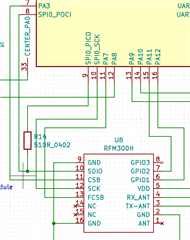
I am connecting to a CMOSTEK CMT2300A RFM300HW HopeRF module. I have to contend with (ref P27/46 CMT2300A_EN_V1.0 manual) "To be noticed, when reading a register, MCU and CMT2300A will have to switch the direction of their IO (SDIO) between the address bit 0 and the data bit 7. It is required that the MCU switches the IO to input mode before send out the falling edge of the SCLK; CMT2300A should switch the IO to output mode after it has seen the falling edge of the SCLK. This avoids data contention of the SDIO (both of the MCU and CMT2300A set the SDIO to output mode at the same time), which would cause unexpected electrical problem."

I have a resistor R14 on the CPU Controller Out line to try and save burning out should the RF module and CPU decide to drive out at the same time.

Excluding bit banging everything, what would be the best way to make this work? I manually drive the SPI chip select(s) in software so it stays enabled as long as I like.

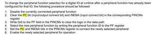
1. Create a timer interrupt that is just shy of the of the time the last bit finishes transmitting, and reconfigure the SPI_PICO pin to an input so it stops driving before the SPI_CLK transitions to enable the RF module to start TX

2. When sending the SPI_PICO register address from the CPU to the RF module, set the frame format to 7 bits to send bits 7 to 1, and then handle the last bit separately in software by re configuring the SPI pins as GPIO and bit banging the last bit before changing to read the register data?

  • I notice that the clock phase is specified (set on falling, fetch on rising) but not the polarity. Notwithstanding the diagrams which suggest CPOL=0, I wonder if you could use CPHA=1, CPOL=1, which would hold off the target (CMT) side indefinitely between bytes. [Compare CMT2300A-Rev0.7 Fig 6 with TRM (SLAU847D) Fig 20-7].

    This almost matches with Microwire, except that line protocol specifies an extra SCLK between request (write) and response (read) which would get in the way.

  • Thank you Bruce, you've given me ideas.Sorry I didn't send this as well before (ref CMT2300A-Rev0.7 manual) "The chip communicates with the outside through the 4-wire SPI interface. The CSB is the active-lowchip select signal for
    accessing to the registers. The FCSB is the active-low select signal for accessing to the FIFO. They cannot be set to low at the
    same time. The SCLK is the serial clock.Its highest speed is 5MHz.The chip itself and the external MCU send the data at the
    falling edge of SCLK and capture the data at the rising edge of SCLK. The SDA is a bidirectional pin for input and output data.
    The address and data are transferred starting from the MSB."

    I wonder what their designers were thinking, as they refer to SDA and SCL similar to I2C nomenclature and have a r/w bit at the start? By trying to make it like SPI they've created an unhappy marriage. Another trap is calling it a 4 wire SPI interface, but it has 2 chip selects instead of 2 unidirectional data lines.

    Whatever I do, I will have to switch the CPU PICO line between Input and Output, and only software can do that I think? Your reply helped me to realize I can switch the PICO line to an input as soon as the RF module reads the last bit, after the rising clock edge. I can guess from the 5MHz max SPI CLK rate it can handle, that the RF module must finish sampling the data line in less than 1/2 that clock period, about 100nS? I can ask HopeRF's tech support if they know the exact time.

    I was thinking I would have to use a timer interrupt, but perhaps I could use the CPU SPI RX interrupt with the FIFO level set to 1 byte, IF the FIFO full interrupt triggers on the rising edge of the last bit reading in (as the CPU SPI is POCI always receiving)? The SPI FIFO RX full interrupt would be better to use than a timer interrupt, as I wouldn't have to (re)calculate timer cycles for a timer interrupt based on SPI clock rate. As long as the SPI RX FIFO interrupt software routine doesn't switch the PICO to an input before 100nSec, it should suit any SPI Clk rate.

  • It is a somewhat unusual bus design.

    Yes, I expect you'll need to do the turnaround in software. That would consist of switching the PF in the PICO pin's PINCM (IOMUX) register from PF=<whatever SPI is for that pin> to PF=1 (GPIO). Sometime before the next transaction, you would set PF=<SPI> again. At startup you would clear the relevant DOE31_0 bit. Thus the pin is either (a) SPI, with the output enabled or (b) GPIO, with the output disabled.

    I agree that 100ns (half a minimum SCK cycle) has to be enough time for it to sample. This is actually quite a short time from your side -- at 32MHz, that's only 4 CPU clocks, and you'll take longer than that to do the switch. For a 5MHz SPI, I expect polling the SPI comes out ahead of interrupts.

    It looks(?) as though the FIFO operations are all unidirectional, so I suppose the "fancy footwork" only applies to register reads.

  • Thanks for confirming I'm on the right track - yes only reading the RF modules registers needs the special SPI_PICO IO pin switching.
    These new MSPM0 MCUs have extensive peripheral config options compared to the old MSP430 I am used to.
    I think I need to disconnect the SPI output from the pin (PC bit), and put it into a high Z state.
    Does "Application software is responsible for ensuring that the IOMUX settings do not conflict..."(ref p733 SLAU847D) mean the MSPM0 can damage itself if incorrectly configured, regardless of external circuitry?
    ref Figure 9-1 and 9.2.1 Peripheral Function (PF) Assignment, it lists separate steps 1-6 of which I would only need to do 1 -3, which may be quicker to execute?
    "When no peripheral function is selected (PF==0) the output latches are put into a reset state, causing the output
    NMOS and PMOS to be disabled (leaving the IO pin in a Hi-Z state with the exception of any enabled pullup/
    pulldown resistors)." ref p735 SLAU847D
    Can I write 0 into the PINCM.PF bits and the PC (Perpheral Connect) at the same time and leave the INENA (Input Connect) bit off?
    I'm not sure if steps can be combined into one fast single write to the PINCM register? I would like to avoid any internal MCU race conditions if there is a risk of blow up of the internal IOMUX circuit, or output of a glitch on the PICO output?

  • I think the "is responsible" comment means "it may not work properly", not "will damage something". I don't know, e.g. what happens if you enable both the pull-up and the pull-down, but I can't imagine it would hurt anything.

    You would do Steps 1-3 to disconnect, then 4-6 to reconnect (though you won't needs steps (1) or (6).

    The TRM mentions (2)/(3) [CONNECTED=0 then PF=0] as separate steps, but I'm not sure that's necessary. Even the driverlib IOMUX functions set all the configuration in a single assignment. 

    You might want to set the internal pullup when disconnecting (but everything else =0), solely to provide an indication on your scope of when the wire is Hi-Z.

    Do you have any equipment yet? I'd want to make sure about the CPOL=1 trick sooner rather than later.

  • Yes not working properly would be a lot better than damaging something. I found the MSP430 usually survived my accidental overcurrent abuse, hopefully this will be as hardy.
    I can follow the TRM:
    IOMUX->SECCFG.PINCM[GPIO_SPI_0_IOMUX_PICO] = GPIO_SPI_0_IOMUX_PICO_FUNC; //Clear the PC bit first, last output state is retained
    IOMUX->SECCFG.PINCM[GPIO_SPI_0_IOMUX_PICO] = 0; // now the peripheral function can be zeroed without risk of ripple through to output as output remains latched when PC = 0
    IOMUX->SECCFG.PINCM[GPIO_SPI_0_IOMUX_PICO] = IOMUX_PINCM_PC_CONNECTED; //Peripheral zero is now "connected" (output logic flip flops now convey HiZ request to driver logic)

    Yes Driverlib doesn't seem to follow the TRM. Perhaps they can get away with it if they assume no one would configure an active peripheral?

    For the SPI clock polarity trick to freeze things just before the RF module switches it's SDIO to output, ref p1243 TRM
    "Clock polarity (CTL0.SPO) is used to control the clock polarity when data is not being transferred and it is only used in the Motorola SPI frame mode."
    Figure 20-7. Motorola SPI Frame Format With SPO = 1 and SPH = 1 looks like it would do as wanted at the last bit holding just before the transition. But then I am not sure how to handle the starting MSB?
    Do you think I should start the SPI off with SPO = 0 and SPH = 0, and then as soon as I have loaded the SPI transmit FIFO, switch it to SPO=1 and SPH = 1 while it is transmitting?

    I now have one prototype hand soldered I can use for testing, with 4 others that can be fitted with RF modules if I blow it up.

  • If the CMT accepts CPOL=1 there's no reason not to use SPO=1/SPH=1 all the time. I suspect it does accept CPOL=1, but this is the kind of thing I like to see in operation before I bet my project on some feature.

    --------------------

    I think your register_read() will look mostly like an ordinary one:

    1) pico_connect()

    2) write TXDATA=request

    3) spin until STAT:RFE=0 [very short time]

    4) read (and throw away) RXDATA [you know what it says]

    5) pico_disconnect()

    6) write TXDATA=dummy

    7) spin until STAT:RFE=0 [very short time]

    8) read result=RXDATA

    Where all you've added are (1) and (5). I personally would leave PICO disconnected most of the time (as above) since I goof frequently, but that's your call.

    [Edit: I suspect you don't need this third line:

    IOMUX->SECCFG.PINCM[GPIO_SPI_0_IOMUX_PICO] = IOMUX_PINCM_PC_CONNECTED; //Peripheral zero is now "connected" (output logic flip flops 

    since "connected to PF=0" ends up being the same (Hi-Z) as "unconnected". See also:

    https://e2e.ti.com/support/microcontrollers/arm-based-microcontrollers-group/arm-based-microcontrollers/f/arm-based-microcontrollers-forum/1467415/lp-mspm0l1306-glitch-generation-when-changing-pf-field-in-pincmx-register-to-0x0/5667370

    notably items (2) [the first one] and (3).]

  • Thank you that has given me some more ideas.
    I am implementing a delay prioritized Listen Before Talk radio protocol. The quicker I can get the RF to transition from receive to transmit, the finer I can make "channel monitor resolution time" for collision avoidance to separate more nodes that are waiting to talk at the same time as soon as the channel becomes free.
    Hence less program steps = faster = more individual time slots in the same LBT period = better collision avoidance.
    To switch from RX to TX, I have to send register write(s) to the HopeRF module.
    Now I see if I have the PICO all set up rearing to go for writing a resister, it will speed things up a little.
    RF module FIFO reading is non-urgent, and so is the register read I do for reading the RSSI strength of the received packet.

    Thanks for that glitch forum thread reference, I am sorry I have difficulty understanding it. Did they somehow generate an output glitch while PC was disconnected just through changing PF? I can't see where they reconnected PC.
    From TRM Figure 9-1. Superset IO Slice, am I correct thinking that PC Connect cleared = "Freeze and Hold Output State"?
    Hence if I did not set PF to zero and then reconnect PC = 1, the FET output driver would remain on and fight with the RF module output?

    Most of the time I will only lower the Chip Select(s) after I have completed SPI PICO IO switching, and also after I have loaded the SPI TX FIFO, so that even if the RF Module now or later versions don't like PICO being high when CS falls it will never see it at the start of a transmission.

  • PC Connect cleared

    Yes, you are right.

    The PMCU indicates to the IOMUX when a peripheral is entering a disabled state via the IORET signal, which is combined with the PC signal via a logic OR to control the output state latches. This mechanism handles preservation of the last valid output state of peripherals in power domain 1 (PD1) when entering STOP or STANDBY mode, as PD1 peripherals are always temporarily disabled upon entry to STOP/STANDBY, and re-enabled upon exit from STOP/STANDBY modes.

    Did they somehow generate an output glitch while PC was disconnected just through changing PF?

    To avoid the glitch, please follow the steps we provided in the TRM to change the PF

  • Hi Gary, back to the SPI interface, I'm trying now in hardware instead of software to change PICO to high impedance after the first 8 bits of a 16 bit transfer have been sent to the HopeRF module. I intend using a timer to trigger a DMA transfer to the PICO IO config to put it in high impedance at the carefully calculated time. Could you help me understand, in the TRM  table 20.3.2 PICO (Offset = 8h) page 1258, it has both a HIGHZ1(bit 25) and HIGHZ0(Bit24). On the IOMUX register for the pin 9.3.1 PINCM (Offset = 4h)page 739, the table is almost the same, but lacks the HIGHZ0(bit24) which is listed as reserved. 

    Question: Do these two configuration registers control the same thing? Or does one of them take priority?

  • I'm not sure I understand the purpose of the timer. Assuming the CPOL=1 trick works you have all the time in the world to put PICO into Hi-Z at the handover.

    The "glitch" in the other thread was not a matter of anything driving low, it was rather that the voltage sagged briefly when the pin went into Hi-Z and the internal pullup was slow to engage. There, the pulled-up state was intended. In your case, the Hi-Z state is what you want.

    I've never seen an explanation for what all those funny registers in the low SPI space (SCLK, CS2_POCI2, et al) are/do. I haven't seen them non-0, and my writes to them are ignored. I think the IOMUX is the place to do all this.

  • Question: Do these two configuration registers control the same thing? Or does one of them take priority?

    No, there are different.

    For HIGHZ1 and HIGHZ0 in PICO to control the output status to Hi-Z Output Mux

    But the HIZ1 in PINCM is to control Z1 as below

    They have the same priority due to they are using or to combine 

  • Thank you Gary, so I can set both HighZ1 and HighZ0 together to make the SPI PICO high Z without disconnecting the SPI peripheral. Is that better than the IOMUX Z1, if Z1 doesn't put the output in to HiZ when the Output Mux DOUT is zero?

  • Hi Bruce, I was a bit nervous about the CPOL=1 method with software juggling, and thought if I can get the hardware to handle the switch to HiZ then my code will be more standard for someone else to follow. Perhaps I can also get the interface to operate at a higher bit rate as well if doing the HiZ transition in hardware? HopeRF's manuals recommend I have the SPI data rate 2 x the speed of radio transmission, which I would like to go as fast as practicable so we can have very large arrays of sensors with least delay communicating to them all. The largest install site of our previous product using the msp430 was a warehouse with 327 light controllers. It still works well. I hope using the mspm0 with more memory I can implement more features. The most complex part is this RF Module communications.

  • Is that better than the IOMUX Z1

    I think  so

    if Z1 doesn't put the output in to HiZ when the Output Mux DOUT is zero?

    Please refer to this table

  • Hi Gary,

    I have problems trying to read the SPI0->PICO register at offset 8.

    I defined:

    unsigned int SPIPICORead;

    then

    As soon as I try to disassembly step over on the ldr r0, [r0] with R0 = 0x40468008, an "unexpected interrupt" occurs, and it jumps here:

    /* This is the code that gets called when the processor receives an unexpected  */
    /* interrupt.  This simply enters an infinite loop, preserving the system state */
    /* for examination by a debugger.                                               */
    void Default_Handler(void)
    {
        /* Enter an infinite loop. */
        while (1) {
        }
    }

    Have I done something wrong?

    Thanks Antony

  • It seems some issue with the CCS and we have report to our tools team will fixed it in future.