Part Number: AM2434
Other Parts Discussed in Thread: SYSCONFIG
Tool/software:
Hi expert,
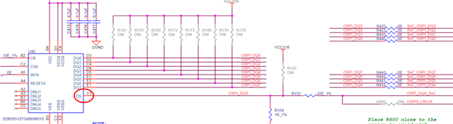
(AM2434 + S28HL512T)
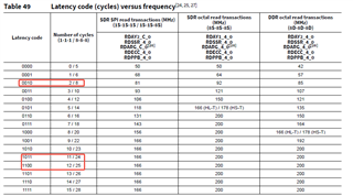
Flash datasheet:
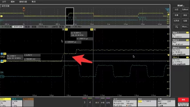
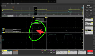
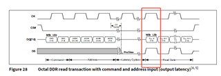
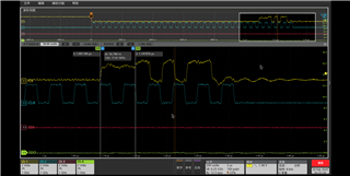
The waveform when reading OSPI flash in 8D mode, found the high level of DQs pins does not reach VDD at the first data bit, as below picture.
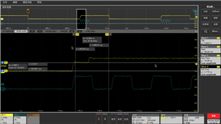
Corresponding to the following mark .
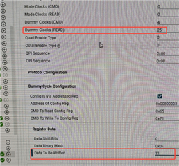
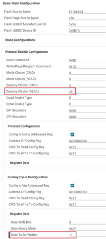
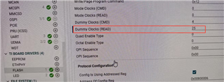
We think it may be due to this config value of sysconfig
Through ospi_flash_diag project, we can read out dummyClksRd = 24 from flash chip, it is exactly one clock less that sysconfig value.
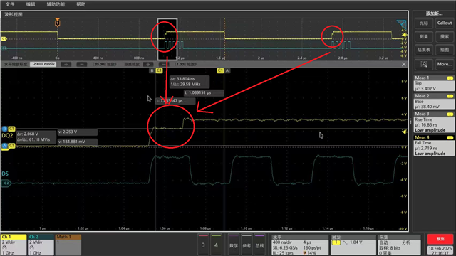
The host delayed a CLK release the DQs pins resulting in a half-level?
As test, change the value to 26, then extend one more CLK half-level, as show in the below picture.
Then change to 24, can't read value from flash correctly.
Now we would like to ask whether our speculation is correct, and how to eliminate this half-level issue?