This thread has been locked.

If you have a related question, please click the "Ask a related question" button in the top right corner. The newly created question will be automatically linked to this question.

LP-MSPM0G3519: How to configure and program unchecked region of DATA flash

Part Number: LP-MSPM0G3519
Other Parts Discussed in Thread: SYSCONFIG

Tool/software:

Hi Team,

I have the example case provided by TI which reads/writes 0x00001000 address.

Now want to try program and read from 0x41E00000 region.

While trying to change it to write starting from 0x41E00000 using the available functions from SDK i am not able to write.

Memory shows ???? in the memory view of CCS, how to use this memory for write and read operations?

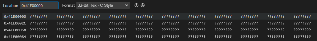
Please support to resolve this

Thanks.

  • Hi Eswaran,

    The memory location 0x41E00000 won't be recognized by the compiler as a valid memory location with the current SysConfig generated linker.

    You'll need to adjust the linker file (.cmd). currently in the SysConfig generated version it will have the Data Memory section starting at 0x41D00000.

    1. Create a new linker file (.cmd extension)
    2. Copy and paste the contents of the SysConfig generated version into your new linker
    3. Edit the origin of the data section to 0x41E00000.
    4. Deselect Linker File Generation in Sysconfig
      1. Project Configuration -> Linker File Generation

    Regards,
    Luke

  • /*****************************************************************************
    
      Copyright (C) 2023 Texas Instruments Incorporated - http://www.ti.com/ 
    
      Redistribution and use in source and binary forms, with or without 
      modification, are permitted provided that the following conditions 
      are met:
    
       Redistributions of source code must retain the above copyright 
       notice, this list of conditions and the following disclaimer.
    
       Redistributions in binary form must reproduce the above copyright
       notice, this list of conditions and the following disclaimer in the 
       documentation and/or other materials provided with the   
       distribution.
    
       Neither the name of Texas Instruments Incorporated nor the names of
       its contributors may be used to endorse or promote products derived
       from this software without specific prior written permission.
    
      THIS SOFTWARE IS PROVIDED BY THE COPYRIGHT HOLDERS AND CONTRIBUTORS 
      "AS IS" AND ANY EXPRESS OR IMPLIED WARRANTIES, INCLUDING, BUT NOT 
      LIMITED TO, THE IMPLIED WARRANTIES OF MERCHANTABILITY AND FITNESS FOR
      A PARTICULAR PURPOSE ARE DISCLAIMED. IN NO EVENT SHALL THE COPYRIGHT 
      OWNER OR CONTRIBUTORS BE LIABLE FOR ANY DIRECT, INDIRECT, INCIDENTAL, 
      SPECIAL, EXEMPLARY, OR CONSEQUENTIAL DAMAGES (INCLUDING, BUT NOT 
      LIMITED TO, PROCUREMENT OF SUBSTITUTE GOODS OR SERVICES; LOSS OF USE,
      DATA, OR PROFITS; OR BUSINESS INTERRUPTION) HOWEVER CAUSED AND ON ANY
      THEORY OF LIABILITY, WHETHER IN CONTRACT, STRICT LIABILITY, OR TORT 
      (INCLUDING NEGLIGENCE OR OTHERWISE) ARISING IN ANY WAY OUT OF THE USE 
      OF THIS SOFTWARE, EVEN IF ADVISED OF THE POSSIBILITY OF SUCH DAMAGE.
    
    *****************************************************************************/
    -uinterruptVectors
    --stack_size=256
    
    /*
     * Note: SRAM on this device is continuous memory but partitioned in the 
     * linker into two separate sections. This is to account for the upper 64kB
     * of SRAM being wiped out upon the device entering any low-power mode 
     * stronger than SLEEP. Thus, it is up to the end-user to enable SRAM_BANK1 for
     * applications where the memory is considered lost outside of RUN and SLEEP Modes.
     */
    
    MEMORY
    {
        FLASH           (RX)  : origin = 0x00000000, length = 0x00080000
        SRAM_BANK0      (RWX) : origin = 0x20200000, length = 0x00010000
        SRAM_BANK1      (RWX) : origin = 0x20210000, length = 0x00010000
        BCR_CONFIG      (R)   : origin = 0x41C00000, length = 0x000000FF
        BSL_CONFIG      (R)   : origin = 0x41C00100, length = 0x00000080
        DATA            (R)   : origin = 0x41E00000, length = 0x00004000
    
    }
    
    SECTIONS
    {
        .intvecs:   > 0x00000000
        .text   : palign(8) {} > FLASH
        .const  : palign(8) {} > FLASH
        .cinit  : palign(8) {} > FLASH
        .pinit  : palign(8) {} > FLASH
        .rodata : palign(8) {} > FLASH
        .ARM.exidx    : palign(8) {} > FLASH
        .init_array   : palign(8) {} > FLASH
        .binit        : palign(8) {} > FLASH
        .TI.ramfunc   : load = FLASH, palign(8), run=SRAM_BANK0, table(BINIT)
    
        .vtable :   > SRAM_BANK0
        .args   :   > SRAM_BANK0
        .data   :   > SRAM_BANK0
        .bss    :   > SRAM_BANK0
        .sysmem :   > SRAM_BANK0
        .TrimTable :  > SRAM_BANK0
        .stack  :   > SRAM_BANK0 (HIGH)
        .eeprom_bss   : palign(8) {} > SRAM_BANK1
        .eeprom_data  : palign(8) {} > SRAM_BANK1
        .BCRConfig  : {} > BCR_CONFIG
        .BSLConfig  : {} > BSL_CONFIG
        .DataBank   : {} > DATA
    }
    

    Hi Luke,

    Thanks for your reply. With the recommended changes I am still facing the same issue. Please verify if what I have done is correct.

    Thanks,

    Eswar G

  • Hi Eswar,

    I'm looking into the issue, I also can't get this to work on my end. The ECC region 0x41D00000 is working fine, but the erase is failing for the unchecked region. I will need to investigate this.

    Are you able to use the ECC region with the ECCGenerated functions?

    DL_FlashCTL_programMemoryFromRAM8WithECCGenerated
    DL_FlashCTL_programMemoryFromRAM16WithECCGenerated
    DL_FlashCTL_programMemoryFromRAM32WithECCGenerated
    DL_FlashCTL_programMemoryFromRAM64WithECCGenerated
  • Hi Luke,

    Thanks for confirming and also for looking into the issue.

    Yes, I have tried using the 0x41D00000 ECC region but with only 64bits write at a time was successful.

    When tried with 32bits function I am getting the first write as successful but when the next 4-byte is being tried to be written at 0x41D00004 the value is overwritten at 0x41D00000. And this happens throughout the 1KB sector. - Still an issue couldn't resolve it.

    Other two functions I haven't tried. Will try to check and let you know. Thanks.

  • The ECC region will need the correct ECC code, so when you do a 32 bit write with ECC generated, it will generate the ECC code for the 32 bits, so it will be correct. BUT, if you then write to the same 64 with another 32 bits, then your ECC code should be different.

    So either, only program 64 bits at a time or ensure you program the ECC properly. You can read a bit more in the paragraph from the TRM below.