This thread has been locked.

If you have a related question, please click the "Ask a related question" button in the top right corner. The newly created question will be automatically linked to this question.

MSPM0G3507: CAN RX with DMA

Part Number: MSPM0G3507
Other Parts Discussed in Thread: SYSCONFIG

Tool/software:

Hi there,

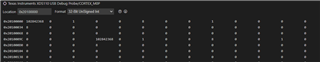
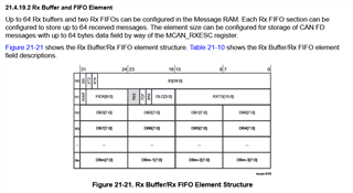
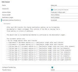
I would like to implement CAN RX with DMA.

Is there any corresponding documentation, tutorials, sysconfig, code examples that I can refer to and learn from?

Unfortunately I have not found much suitable.

Thanks a lot in advance.

Matze

  • Hi Matze,

    We don't have an exact CAN DMA example but you can take the basic CAN examples and add the DMA to move the data between buffers. The important part is to correctly configure the DMA to handle the transfer of data from your source to destination.

    For RX the source will be the CAN RX register and the destination will be some buffer/array that you setup to receive the data. Number of transfers should be the size of your expected message divided by the packet size. You will want to increment the destination address but not the source.

    TX is the exact opposite with the source incrementing and the destination remaining the same. Number of transfers and size will be the same ideology. 

    I recommend on the RX side to trigger your DMA from the CAN RX interrupt (use the event system).

    Examples to check out:

    • mcan_multi_message_tx
    • mcan_message_rx
    • For DMA interactions
      • uart_tx_multibyte_fifo_dma_interrupts
      • uart_rx_multibyte_fifo_interrupts

    Regards,
    Luke

  • Thanks!

    For the RX source I think I have to use the RX FIFO0 Start Address 172

    Because I am using

    Filter Element Configuration Store in Rx FIFO 0 if filter matches

    But when I look into the Memory view I only see the following:

    _____________________________________________________________________________________________________________________________________

    1st issue about the memory view:

    Address 192 is occupied by "DL_MCAN_msgRAMConfig" even though I configured 10 FIFO0 elements and the FIFO0 should end at 332, not 192.

    _____________________________________________________________________________________________________________________________________

    2nd issue about the memory view:

    When I receive a CAN message it doesn't show in the memory view. All values stay unchanged. The receiving itself does work because the message appears in my rxMsg-Struct. But why don't I see it in memory view?

    _____________________________________________________________________________________________________________________________________

    EDIT: I'm afraid I got RAM and ROM mixed up. Did I? I configure the adresses for the FIFO0 elements in the RAM. The memory view shows the ROM, right?

    Is there any possibility to view the contents of the message RAM FIFO?

    And how do I instruct the DMA to reference the RAM and not the ROM when I specify the source address?

    _____________________________________________________________________________________________________________________________________

    uart_rx_multibyte_fifo_interrupts

    I checked out this example and tried to adapt the implementation of the DMA from this example project to my project.

    I added the following lines to my main_msp***.c:

    volatile uint8_t gRxDataframe[16];
    
    int main(void)
    {
        SYSCFG_DL_init();
    
      /* Configure DMA source, destination and size */
        DL_DMA_setSrcAddr(DMA, DMA_CH0_CANRX_CHAN_ID, (uint32_t)(CAN_Info.gMCAN0MsgRAMConfigParams.rxFIFO0startAddr));
        DL_DMA_setDestAddr(DMA, DMA_CH0_CANRX_CHAN_ID, (uint32_t) &gRxDataframe[0]);
        DL_DMA_enableChannel(DMA, DMA_CH0_CANRX_CHAN_ID);
    
        /* Confirm DMA channel is enabled */
        while (false == DL_DMA_isChannelEnabled(DMA, DMA_CH0_CANRX_CHAN_ID)) {
            __BKPT(0);
        }
    
        NVIC_EnableIRQ(MCAN0_INST_INT_IRQN);
    
        gCheckCAN = false;
    
        DL_SYSCTL_disableSleepOnExit();
        /* Wait in SLEEP mode until DMA interrupt is triggered */
        while (false == gCheckCAN) {
            __WFE();
        }
    
        DL_SYSCTL_enableSleepOnExit();

    And I made the following changes to the sysconfig:

    DMA.associatedChannels.create(1);
    DMA.associatedChannels[0].addressMode           = "f2b";
    DMA.associatedChannels[0].srcLength             = "BYTE";
    DMA.associatedChannels[0].dstLength             = "BYTE";
    DMA.associatedChannels[0].configureTransferSize = true;
    DMA.associatedChannels[0].transferMode          = "FULL_CH_REPEAT_BLOCK";
    DMA.associatedChannels[0].transferSize          = 16;
    DMA.associatedChannels[0].destIncrement         = "INCREMENT";
    DMA.associatedChannels[0].enableInterrupt       = true;
    DMA.associatedChannels[0].$name                 = "DMA_CH0_CANRX";
    DMA.associatedChannels[0].peripheral.$assign    = "DMA_CH0";

    What else do I have to do?

    _____________________________________________________________________________________________________________________________________

    I recommend on the RX side to trigger your DMA from the CAN RX interrupt (use the event system).

    I tried many different possibilities but I couldn't find any solution in the sysconfig how to link the CAN Rx Interrupt to the DMA as a trigger by any connection via event system. Please help me to understand this and to find the right way to this configuration.

    I had the idea that DL_DMA_startTransfer() might be the function that I was looking for.

    I added it to my CAN RX interrupt but I don't see any data in my watch expression "gRxDataframe"  after the CAN_Rx_Interrupt and the execution of DL_DMA_startTransfer() .

    Thanks a lot in advance!

    Matze

  • Hi Matze,

    The DMA setup looks correct for the RX, I don't see the number of transfers set, so make sure you have the correct number with regards to how much data you're transferring per transfer. I had to double check, but the CAN module only has CPU interrupts, so your process is correct of creating the Interrupt Handler to start the DMA transfer when you get the RX interrupt.

    The memory address you have shown is not ROM though, that is the normal flash region. I'm looking into what address space you need to view to see the RX CAN buffer.

    Regards,
    Luke

  • Hi and thanks!

    I don't see the number of transfers set, so make sure you have the correct number with regards to how much data you're transferring per transfer.

    What do you mean by "number of transfers"?

    _____________________________________________________________________________________________

    I'm looking into what address space you need to view to see the RX CAN buffer.

    Thanks, I quickly found my CAN RX FIFO0 in address 0x2010.0000. I can see every CAN Msg that I receive in the memory starting from this address.

    I am wondering why every CAN frame takes 42 * 32Bit in this memory.

    According to this Figure 21-21 I would have expected a size of 4 * 32Bit for one CAN Frame with 8 Data Bytes.

    Please clarify ;)

    _____________________________________________________________________________________________

    And just another short question: is there any possibility to adjust the view so that I see each new message in a new line, i.e. a line break after each CAN frame in this memory view?

    _____________________________________________________________________________________________

    I also see the &gRxDataframe[0], the destination for the DMA-Transfer, in the memory view. But the memory values stay "0" even though I receive a CAN message, see it in the FIFO memory view and - debugged via breakpoint - that the                 "DL_DMA_startTransfer(DMA, DMA_CH0_CANRX_CHAN_ID);" got executed.

    Any idea what I am missing? What might still go wrong?

    Thanks a lot in advance! Best regards!

    Matze

  • Hi Matze,

    The number of transfers will be the DMASZ bit, transfers should be Size of Total data needing to be transferred / size of the transfer (byte, word, 2 words etc.).

    Your data does look strange here, it looks like you're storing only 1 bit in a whole 32-bit int, unless your data should only be 1 or 0...

    For the element address you should look at how the DL_MCAN_readMsgRam() function is created (located in dl_mcan.c). I'll break it down a bit but I do recommend looking at the function, essentially you'll need to follow the FIFO path and instead of the readMsg function you'll use the DMA with the elemAddr as your source address and the buffer as your destination address.

    The MCAN packet has a bunch of header information then the data as you see in the element structure. The DL_MCAN_readMsg function will break down all the bits and put them into the correct organization where as the DMA will only pull the data directly from the registers. So you need to structure your transfers to transfer and increment all the data in multiples of your expected packets. The increment and transfer sizes should be used to span across your whole expected data set

    ----

    /*Start Addr intitial value is from your MCAN_RXF0C_F0SA setting
    ElemSize inital value is from your MCAN_RXESC_F0DS
    idx is from your MCAN_RXF0S_F0GI setting*/
    
    
    startAddr = (uint32_t)(startAddr << 2U);
    elemSize  = DL_MCAN_getMsgObjSize(elemSize);
    elemSize *= 4U;
    elemAddr = startAddr + (elemSize * idx);
    elemAddr += MCAN_MCAN_MSG_MEM;
    DL_MCAN_readMsg((uint32_t) mcan, elemAddr, elem);