Part Number: MSPM0L1106
Other Parts Discussed in Thread: LP-MSPM0L1306, SYSCONFIG
Tool/software:
Hi Teams,
During testing on my MSPM0L1106 PCBA, I had the following questions and please help to provide me suggestion and solution :
Question 1 :
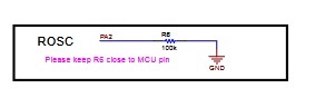
- MCU VDD = 1.8V
- A protential divider with upper R1=220K and lower R2=100K to GND.
- MCU PA2 is connected to the connection between R1 and R2.
- PA2 is configured as input without any pull resistor.
By using software and multi-meter to measure on PA2, the result are 0 and 0V respectively. When 5V is applied to R1, the same result is obtained. The expected result should be 1 and ~1.56V.
When R1 is changed to 22K, the measured result will be 1 and ~1.6V respectively. What is the cause of the problem? (Remark: this circuit is working with other MCU, 8051 core.)
Question 2 :
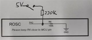
With the same software in Q1 above, I tested on LP-MSPM0L1306 LaunchPad.
Added 220K resistor to 5V and R6 on the board. Although the VDD is 3.3V on LaunchPad, but the voltage on R6 is 0V too.
- By using the original LaunchPad and the firmware in Q1, I added following code to setup PA2 as input with pull up resistor after system initialized and measure the voltage on R6. The voltage is close to 0 too and I was expecting certain voltage. What is the cause of it?
DL_GPIO_initDigitalInput(GPIO_PA_PA2_IOMUX);
DL_GPIO_initDigitalInputFeatures( GPIO_PA_PA2_IOMUX, DL_GPIO_INVERSION_DISABLE, DL_GPIO_RESISTOR_PULL_UP, DL_GPIO_HYSTERESIS_DISABLE, DL_GPIO_WAKEUP_DISABLE );
- If the code is changed to setup PA2 as output high after system initialised adn measure the voltage on R6. The voltage is close to 0 too and I was expecting 3.3V, What is the cause of it?
DL_GPIO_initDigitalOutput(GPIO_PA_PA2_IOMUX);
DL_GPIO_setPins(GPIO_PA_PORT, GPIO_PA_PA2_PIN);
Question 3 :
Based on Q2, I test on PA3 again. PA3 is configured as output low in .syscfg.
- PA3 is setup as input with pull up resistor after system initialized and measure the voltage on PA3 (header J2). The voltage is close to 0 too and I was expecting 3.3V. What is the cause of it?
DL_GPIO_initDigitalInput(GPIO_PA_PA3_IOMUX);
DL_GPIO_initDigitalInputFeatures( GPIO_PA_PA3_IOMUX, DL_GPIO_INVERSION_DISABLE, DL_GPIO_RESISTOR_PULL_UP, DL_GPIO_HYSTERESIS_DISABLE, DL_GPIO_WAKEUP_DISABLE );
- PA3 is setup as output high, 3.3V can be meaured.
Question 4 :
I notice that the generated function, SYSCFG_DL_GPIO_init(), do not have the code, "DL_GPIO_initDigitalInput(GPIO_PA_PA2_IOMUX);" for PA2 as an input. Is this correct? (Remark: Other input GPIOs have the corresponding lines.)
AlanC.