Part Number: MSPM0G3507-Q1
Other Parts Discussed in Thread: ADS8688, MSPM0G3507
Tool/software:
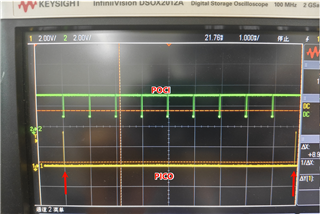
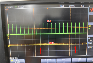
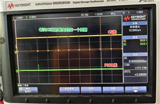
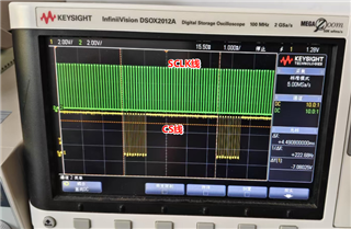
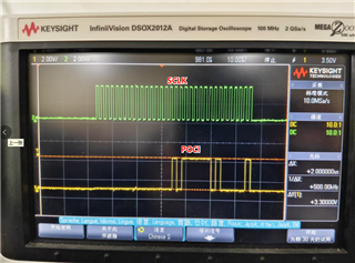
I am currently using the SPI function of the MSPM0G3507-Q1 chip; The following is my function introduction, I set MSPM0G3507-Q1 as the host, set ADS8688 as the slave, the host sends the command code (0x00000000,0xA0000000), the data is collected from the slave machine and returned to the host. This is the process I expected, but during use, I could not receive the data returned by the machine (to be precise, I set the receive interrupt in the program, and added the breakpoint verification in the interrupt, entering the interrupt is normal, but I can not read the data in the RxData register, I detected the status of RXFIFO, I can not read the data in the RXdata register. It appears as non-empty). I used oscilloscope PICO, POCI, CLK, CS pins in the slave machine to display whether the waveform was correct. What are the reasons for this? How to deal with it?
Below is part of my program code and oscilloscope picture
//Initial configuration of SPI
void SPI0_INIT()
{
//设置时钟源和分频
mySPI0->CLKSEL.bit.SYSCLK_SEL=1;
mySPI0->CLKDIV.bit.RATIO=0;
mySPI0->CTL0.bit.CSSEL=1; //CS线的选择
mySPI0->CTL0.bit.DSS=0xF; //数据尺寸
mySPI0->CTL0.bit.SPH=1; //极性相位
mySPI0->CTL0.bit.SPO=0;
mySPI0->CTL0.bit.FRF=1; //传输帧格式,
mySPI0->CTL1.bit.PES=0; //偶数奇偶校验模式
mySPI0->CTL1.bit.CP=1; //控制器或外设模式选择
mySPI0->CTL1.bit.PTEN=0; //发送奇偶校验
mySPI0->CTL1.bit.PREN=0; //接收奇偶校验
mySPI0->CTL1.bit.MSB=1; //传输的开始端,高位优先
//串行时钟分频器:用于产生SPI的发送和接收比特率
mySPI0->CLKCTL.bit.SCR=0xE;
//设置RX和TX FIFO中断阈值级别
mySPI0->IFLS.bit.RXIFLSEL=0x2;
mySPI0->IFLS.bit.TXIFLSEL=0x2;
//使能接收中断
//mySPI0->C_IMASK.reg=0xFF;
//mySPI0->C_IMASK.bit.TXEMPTY=1;
mySPI0->C_IMASK.bit.IDLE=1;
mySPI0->C_IMASK.bit.RX=1;
//mySPI0->C_IMASK.bit.RXFULL=1;
//mySPI0->C_IMASK.bit.DMA_DONE_RX=1;
//使能
mySPI0->CTL1.bit.ENABLE=1;
}
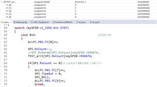
//Interrupt part
switch (mySPI0->C_IIDX.bit.STAT)
{
case 0x4: //接收中断
{
ALLFC.P01.FC[10]++;//mySPI0->C_IMASK.reg;
SPI.RxCount--;
SPI.RxDataW[SPI.RxCount]=mySPI0->RXDATA;
if(SPI.RxCount==0)
{
ALLFC.P01.FC[11]++;
SPI.TimeOut=0;
SPI_RX();
}
break;
}
//Sending part
void SPI_TX32(Uint32 _Data) //SPI发送函数
{
if(SPI.Busy) return;
SPI.TxD32=_Data;
SPI.TxCount=2;
SPI.RxCount=2;
mySPI0->TXDATA = SPI.TxDataW[1];
mySPI0->TXDATA = SPI.TxDataW[0];
SPI.Busy=5;
}