


Tool/software:
Hi, I've been reading the AM263x TRM revision H section 6.4 on Clocking. I've noticed the following inconsistencies. Please correct me if I have made the wrong assumptions:
Figure 6-22:
Two different signals are labelled "DPL_CORE_HSDIV0_CLKOUT1". I assume the 192MHz instance should be labeled DPLL_PER_HSDIV0_CLKOUT1?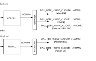
6.4.7.2.4 MCSPI CLOCK:
The steps to cofingure this clock at 50MHz say to use CLKDIV = "3" and CLKSRCSEL = "4" (DPLL_CORE_HSDIV0_CLKOUT0). However Table 6-28 shows DPLL_CORE_HSDIV0_CLKOUT0 has 400MHz frequency, so I think these registers would set configure this clock to 400Mhz/4=100MHz. I asume that I should use to use CLKDIV = "3" and CLKSRCSEL = "2" (SYS_CLK 200MHz) to configure this clock to 50MHz?
6.4.7.2.10 CPTS Clock:
This section says "Update the CPTS GCM register with the value of 0x333 to select PLL_PER_CLKOUT1 as its source, MSS_RCM.CPTS_CLK_SRC_SEL.CLKSRCSEL = 0x333". However Table 6-31 shows that for CPTS, CLKSRCSEL=3 maps to DPLL_CORE_HSDIV0_CLKOUT1. I assume that the quoted sentence means to say "DPLL_CORE_HSDIV0_CLKOUT1 as its source" instead?
