This thread has been locked.

If you have a related question, please click the "Ask a related question" button in the top right corner. The newly created question will be automatically linked to this question.

AM2612: custom flash adaption

Part Number: AM2612
Other Parts Discussed in Thread: SYSCONFIG, LP-AM263, , UNIFLASH

Tool/software:

Hi all:

I am currently working with the LP-AM2612 to debug the ospi_flash_dma example and encountered an issue requiring your expertise. Here are the details:

  1. Original JSON Issue

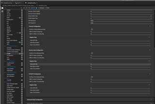
    • Generated a device configuration JSON using the ospi_flash_diag diagnostic example.

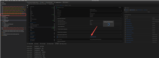
    • Attempted to import the JSON into CCS v20, but the import process hangs indefinitely (continuously "spinning").

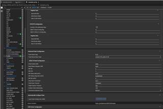
  2. Manual Configuration Attempt

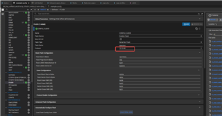
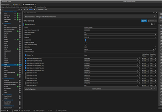
    • Proceeded to manually configure the OSPI Flash parameters based on the JSON content.

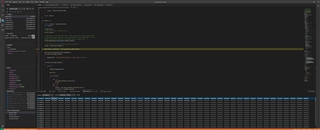
    • However, during debugging, no signal activity is observed on the OSPI interface (confirmed via logic analyzer).

Request:
Could you please:

  • Verify if the ospi_flash_diag JSON generation/import process is compatible with CCS v20?

  • Provide a validated OSPI Flash configuration on syscfg for the LP-AM2612?

Best regards

zx

  • Hi all:

    One more question to add, what is the relationship between the output clock frequency of OSPF and the input clock frequency configured by Syscfg, and why do I use the ospi_flash_diag routine to output ospi_clk 2.5MHz

    Looking forward to your reply

    zx

  • Hi Zx,

    Thank you for the query.

    1. mcu_plus_sdk support is not yet completely integrated with CCS20 versions. Please use CCS 12.8.1 and SysConfig 1.22.0
    2. Load from JSON feature has a KNOW ISSUE will be fixed in the next mcu_plus_sdk 10.2  release for AM261x  2nd week of May.
      1. As a workaround you can modify the flash_am261x.syscfg file in the path: C:\ti\mcu_plus_sdk_am261x_10_00_01_10\source\sysconfig\board\.meta\flash
      2. Changing the flash json path in this file help SysConfig to change the default flash.
      3. Reimport the project
    3. As is see the Flash part used is IS25LX064. This part works in 3.3 domain. LP-AM263 by default functions in 1.8 domain. In this case you will have to change the PMIC LDO voltage from VSYS1V8 to VSYS3V3. 
      1. Driver path :  C:\ti\mcu_plus_sdk_am261x_10_00_01_10\source\board\pmic\pmic_lld\derby\test\power_test.c
      2. pmic_user_reg_cfg example project will be release as part of next release
    4. If this change is done then all the current VSYS1V8 nets will have 3V3 voltage. 
      1. In this ADC refernce voltage should should be provided externally through ADC_EXT_VREF .

    Also the can you please let us know the reason on switching to 3.3V? I belive,1.8V domain flashes are more readily available in market.


    Thanks & Regards,
    Rijohn

  • Hi Rijohn:

      Thanks for your reply.

      1. I am using the original hardware of the development board, and the flash has not been replaced. I wrote the wrong name for Flash. I will make the modifications according to your suggestions. Additionally, there is another question regarding the output clock frequency of OSPI, which is included in the second question

     2. Also, “the flash_am261x.syscfg file”,  is the file modification applicable to our own hardware? Our hardware uses S25FL128LAGBHM023, can this JSON only be manually configured in syscfg

    Best Regards

    zx

  • Hi zx,

    In order for the the flash to work at a frequency close to the input clock frequency = 133MHz then we need to enable the PHY mode. (FYI, This will be enabled in 10.2 releasein ospi_flash_io example)

    In case of ospi_flash diag example OPSI is by default in NON-PHY mode of operation.
    In NON-PHY mode of operation OUTPUT_clock frequency of OSPI = INPUT_clock frequency/ Input Clock divider.

    Minimum value of diver incase of SDR = 4
    Minimum value of diver incase of DDR = 8

    For more information regarding PHY and NON-PHY mode of operation please refer to AM261x TRM OSPI chapter 

    Regards,
    Rijohn

  • Hi Rijohn:

     I have installed CCS12.8. When I import project, CCS reports an error. How can I configure it to work properly.

    The SDK I imported is mcu_plus_sdk_am261x_10_00_01_10.

    Best regards

    zx

  • Hi zx,

    Can you please do the below steps:

    1. After installing CCS 12.8.1 and SysConfig 1.22.0
    2. Navigate to 'Check for updates' in Help tab in CCS and see if there are any pending updates for "Sitara MCU Device" 
    3. After installing the updates, navigate to below in Windows tab in CCS menu : Preferences-> Code Composter Studio->Products
      1. click on Refresh
      2. Then click on "Apply and close"
    4. Restart the CCS and try importing again

    Thanks & Regards,
    Rijohn

  • Hi Rijohn:

     Thanks for your reply.

     I have configured the ccs12.8.

     I want to know how to change the PMIC LDO voltage from VSYS1V8 to VSYS3V3. 

     The reason why I used 3.3 is that I replaced the flash with W25Q256JV, which requires 3.3V power supply. The flash we actually use also requires 3.3V power supply. Also, I would like to know how to change the voltage of the MCU's OSPI pin to 3.3V after changing PMIC LDO voltage

    Best regards

    zx

  • Hi z x,

    Please use  CCS 12.8.1 for AM261x.

    I want to know how to change the PMIC LDO voltage from VSYS1V8 to VSYS3V3

    In this case you will have to change the PMIC LDO voltage from VSYS1V8 to VSYS3V3. 

    1. Driver path :  C:\ti\mcu_plus_sdk_am261x_10_00_01_10\source\board\pmic\pmic_lld\derby\test\power_test.c
    2. pmic_user_reg_cfg example project will be release as part of next release


    Thanks & Regards,
    Rijohn

  • Hi Rijohn:

    I am encountering an issue while adapting our hardware’s Flash( S25FL128LAGBHM023) configuration for the AM2612 processor and would appreciate your guidance.

    Problem Description:

    1. When configuring the OSPI Flash protocol to 1s1s4s, the AM2612 incorrectly sets the mode to 1s4s4s.

      • The OSPI_FLASH_CFG_DEV_INSTR_WR_CONFIG_REG Register[13:12] and OSPI_FLASH_CFG_DEV_INSTR_RD_CONFIG_REG Register [13:12] are both set to 0x02 (indicating 4s mode) instead of the expected 0x01 (1s mode).

      • Temporary Fix in ospi_flash_dma Example: Manually modifying these register bits resolved the issue.

    2. Issue Persists in sbl_jtag_uniflash Example:

      • Despite manually updating the OSPI_FLASH_CFG_DEV_INSTR_WR_CONFIG_REG Register [13:12] to 0x00 , the configuration does not take effect.

      • Confirmed via CCS Memory view that the register value remains unchanged or reverts after modification.

    Questions:

    • Why does the manual register modification work in the ospi_flash_dma example but fail in sbl_jtag_uniflash?

    • Could there be a configuration override or timing issue in the SBL bootloader flow?

    Additional Context:

    • Mcu: XAM2612AODFHMZCZQ1

    • Sdk: mcu_plus_sdk_am261x_10_00_01_10

    • Register Addresses:

      • OSPI_FLASH_CFG_DEV_INSTR_WR_CONFIG_REG Register: [address, 0x53808008]

      • OSPI_FLASH_CFG_DEV_INSTR_RD_CONFIG_REG Register: [Insert address, 0x53808004]

    • The attachment is syscfg
    • Manually modified code is called after Board_driversOpen()
      • int32_t OSPI_lld_norFlashInit1s1s4s(OSPILLD_Handle handle)
        {
            int32_t status = OSPI_SYSTEM_SUCCESS;
            volatile uint32_t regVal = 0U;
        
            /* Check if the handle is NULL */
            if(NULL != handle)
            {
                const CSL_ospi_flash_cfgRegs *pReg = (const CSL_ospi_flash_cfgRegs *)(handle->baseAddr);
                
                /* Wait for a while */
                // uint32_t waitMicro = 500U * 1000U;
                // handle->Clock_usleep(waitMicro);
        
                /* SDR will be enabled in flash by default, set OSPI controller to 1S-1S-1S mode */
                uint32_t xferLines = 0;
        
                /* Set RD and WR Config register */
                regVal = CSL_REG32_RD(&pReg->DEV_INSTR_RD_CONFIG_REG);
                /* Configure the Device Read Instruction Configuration Register */
                regVal &= ~(CSL_OSPI_FLASH_CFG_DEV_INSTR_RD_CONFIG_REG_INSTR_TYPE_FLD_MASK              | \
                            CSL_OSPI_FLASH_CFG_DEV_INSTR_RD_CONFIG_REG_RD_OPCODE_NON_XIP_FLD_MASK       | \
                            CSL_OSPI_FLASH_CFG_DEV_INSTR_RD_CONFIG_REG_ADDR_XFER_TYPE_STD_MODE_FLD_MASK | \
                            CSL_OSPI_FLASH_CFG_DEV_INSTR_RD_CONFIG_REG_DATA_XFER_TYPE_EXT_MODE_FLD_MASK | \
                            CSL_OSPI_FLASH_CFG_DEV_INSTR_RD_CONFIG_REG_DDR_EN_FLD_MASK                  | \
                            CSL_OSPI_FLASH_CFG_DEV_INSTR_RD_CONFIG_REG_DUMMY_RD_CLK_CYCLES_FLD_MASK);
                regVal |= (((uint32_t)0x6B) << CSL_OSPI_FLASH_CFG_DEV_INSTR_RD_CONFIG_REG_RD_OPCODE_NON_XIP_FLD_SHIFT)        | \
                        ((xferLines + 2) << CSL_OSPI_FLASH_CFG_DEV_INSTR_RD_CONFIG_REG_DATA_XFER_TYPE_EXT_MODE_FLD_SHIFT) | \
                        ((xferLines) << CSL_OSPI_FLASH_CFG_DEV_INSTR_RD_CONFIG_REG_ADDR_XFER_TYPE_STD_MODE_FLD_SHIFT) | \
                        ((xferLines) << CSL_OSPI_FLASH_CFG_DEV_INSTR_RD_CONFIG_REG_INSTR_TYPE_FLD_SHIFT)          | \
                        (8U << CSL_OSPI_FLASH_CFG_DEV_INSTR_RD_CONFIG_REG_DUMMY_RD_CLK_CYCLES_FLD_SHIFT);
                CSL_REG32_WR(&pReg->DEV_INSTR_RD_CONFIG_REG, regVal);


                xferLines = 0;
                regVal = CSL_REG32_RD(&pReg->DEV_INSTR_WR_CONFIG_REG);
        
                /* Configure the Device Write Instruction Configuration Register */
                regVal &= ~(CSL_OSPI_FLASH_CFG_DEV_INSTR_WR_CONFIG_REG_DUMMY_WR_CLK_CYCLES_FLD_MASK     | \
                            CSL_OSPI_FLASH_CFG_DEV_INSTR_WR_CONFIG_REG_WR_INSTR_RESV3_FLD_MASK          | \
                            CSL_OSPI_FLASH_CFG_DEV_INSTR_WR_CONFIG_REG_WR_OPCODE_FLD_MASK               | \
                            CSL_OSPI_FLASH_CFG_DEV_INSTR_WR_CONFIG_REG_DATA_XFER_TYPE_EXT_MODE_FLD_MASK | \
                            CSL_OSPI_FLASH_CFG_DEV_INSTR_WR_CONFIG_REG_ADDR_XFER_TYPE_STD_MODE_FLD_MASK | \
                            CSL_OSPI_FLASH_CFG_DEV_INSTR_WR_CONFIG_REG_DUMMY_WR_CLK_CYCLES_FLD_MASK);
                regVal |= (((uint32_t)0x02) << CSL_OSPI_FLASH_CFG_DEV_INSTR_WR_CONFIG_REG_WR_OPCODE_FLD_SHIFT) | \
                        (xferLines << CSL_OSPI_FLASH_CFG_DEV_INSTR_WR_CONFIG_REG_ADDR_XFER_TYPE_STD_MODE_FLD_SHIFT) | \
                        ((xferLines) << CSL_OSPI_FLASH_CFG_DEV_INSTR_WR_CONFIG_REG_DATA_XFER_TYPE_EXT_MODE_FLD_SHIFT);
        
                CSL_REG32_WR(&pReg->DEV_INSTR_WR_CONFIG_REG, regVal);
        
                /* Set read capture delay */
                // status += OSPI_lld_setRdDataCaptureDelay(handle, 0);
            }
            else
            {
                status = OSPI_SYSTEM_FAILURE;
            }
        
            return status;
        }

    Please let me know if further details are required. Thank you for your support!

    This issue is urgent, please follow up as soon as possible

    Best regard

    zx

  • Hi zx, 

    Allow me to check this and get back to you soon.

    Regards,

    Aswin

  • Hi zx, 

    Can you attach a screen snip of your sysconfig OSPI configuration?

    Regards,

    Aswin

  • Hi Aswin,

    Best regards

    zx

  •  

    /*
     *  Copyright (C) 2021-24 Texas Instruments Incorporated
     *
     *  Redistribution and use in source and binary forms, with or without
     *  modification, are permitted provided that the following conditions
     *  are met:
     *
     *    Redistributions of source code must retain the above copyright
     *    notice, this list of conditions and the following disclaimer.
     *
     *    Redistributions in binary form must reproduce the above copyright
     *    notice, this list of conditions and the following disclaimer in the
     *    documentation and/or other materials provided with the
     *    distribution.
     *
     *    Neither the name of Texas Instruments Incorporated nor the names of
     *    its contributors may be used to endorse or promote products derived
     *    from this software without specific prior written permission.
     *
     *  THIS SOFTWARE IS PROVIDED BY THE COPYRIGHT HOLDERS AND CONTRIBUTORS
     *  "AS IS" AND ANY EXPRESS OR IMPLIED WARRANTIES, INCLUDING, BUT NOT
     *  LIMITED TO, THE IMPLIED WARRANTIES OF MERCHANTABILITY AND FITNESS FOR
     *  A PARTICULAR PURPOSE ARE DISCLAIMED. IN NO EVENT SHALL THE COPYRIGHT
     *  OWNER OR CONTRIBUTORS BE LIABLE FOR ANY DIRECT, INDIRECT, INCIDENTAL,
     *  SPECIAL, EXEMPLARY, OR CONSEQUENTIAL DAMAGES (INCLUDING, BUT NOT
     *  LIMITED TO, PROCUREMENT OF SUBSTITUTE GOODS OR SERVICES; LOSS OF USE,
     *  DATA, OR PROFITS; OR BUSINESS INTERRUPTION) HOWEVER CAUSED AND ON ANY
     *  THEORY OF LIABILITY, WHETHER IN CONTRACT, STRICT LIABILITY, OR TORT
     *  (INCLUDING NEGLIGENCE OR OTHERWISE) ARISING IN ANY WAY OUT OF THE USE
     *  OF THIS SOFTWARE, EVEN IF ADVISED OF THE POSSIBILITY OF SUCH DAMAGE.
     */
    #include <stdio.h>
    #include <stdlib.h>
    #include <string.h>
    #include <kernel/dpl/DebugP.h>
    #include "ti_drivers_open_close.h"
    #include "ti_board_open_close.h"
    #include <drivers/bootloader/bootloader_uniflash/bootloader_uniflash.h>
    #include <drivers/ospi/v0/lld/ospi_lld.h>
    #include <drivers/hw_include/cslr.h>
    
    #define FILE_MAX_SIZE   (0x140000) /* This has to match the size of MSRAM_1 section in linker.cmd */
    uint8_t gFileBuf[FILE_MAX_SIZE] __attribute__((aligned(128), section(".bss.filebuf"))); 
    
    #define VERIFY_BUF_MAX_SIZE (32*1024)
    uint8_t gVerifyBuf[VERIFY_BUF_MAX_SIZE] __attribute__((aligned(128), section(".bss")));
    
    #define INPUT_STR_MAX_LEN   (16u)
    static char inputStr[INPUT_STR_MAX_LEN];
    
    #define FILE_NAME_MAX_LEN   (384u)
    
    /* Some common NOR XSPI flash commands */
    #define OSPI_NOR_CMD_RDID           (0x9FU)
    #define OSPI_NOR_CMD_RSTEN          (0x66U)
    #define OSPI_NOR_CMD_RST            (0x99U)
    #define OSPI_NOR_CMD_WREN           (0x06U)
    #define OSPI_NOR_CMD_RDSR           (0x05U)
    #define OSPI_NOR_CMD_RDSFDP         (0x5AU)
    
    #define OSPI_NOR_SR_WIP             (1U << 0U)
    
    #define OSPI_NOR_SFDP_DC            (8U)
    
    #define OSPI_NOR_WRR_WRITE_TIMEOUT  (600U*1000U)
    
    static uint8_t gNorRdCmd = 0x03;
    static uint8_t gNorWrCmd = 0x02;
    static uint8_t gNorErCmd = 0xD8;
    
    static char filename[FILE_NAME_MAX_LEN];
    
    void flashFixUpOspiBoot(OSPI_Handle oHandle);
    void gpio_flash_reset(void);
    void custom_protocol_setting(void);
    int32_t OSPI_lld_norFlashInit1s1s4s(OSPILLD_Handle hOspi);
    
    char gMainMenu[] = {
        " \r\n"
        " \r\n"
        " ==================\r\n"
        " JTAG Uniflash Menu\r\n"
        " ==================\r\n"
        " \r\n"
        " 1: Erase Complete Flash\r\n"
        " 2: Write File to Flash and Verify\r\n"
        " 3: Verify file in Flash\r\n"
        " \r\n"
        " x: Exit\r\n"
        " \r\n"
        " Enter Choice: "
    };
    
    int32_t sbl_jtag_uniflash_load_file(char optype)
    {
        int32_t status = SystemP_SUCCESS;
        uint32_t offset;
        uint32_t fileSize;
        uint32_t eraseBlkSize;
        uint32_t flashSize;
        FILE *fp;
    
        DebugP_log("\r\n");
        DebugP_log(" Enter file name along with path to write or verify : ");
        gets(filename);
        fp = fopen(filename, "rb");
        if(fp == NULL)
        {   /* if file not present then exit */
            DebugP_log(" [FLASH WRITER] Unable to open file %s !!!\r\n", filename);
            status = SystemP_FAILURE;
        }
        if(status==SystemP_SUCCESS)
        {   /* if file size > buffer size then exit, we will load the file in one shot so
             * so file size has to be < buffer size
             */
            fseek(fp, 0, SEEK_END); 
            fileSize = ftell(fp);
            fseek(fp, 0, SEEK_SET);
            fclose(fp);
    
            if(fileSize > FILE_MAX_SIZE)
            {
                DebugP_log(" [FLASH WRITER] File is too large to flash !!!\r\n");
                status = SystemP_FAILURE;
            }
        }
        if(status==SystemP_SUCCESS)
        {
            DebugP_log(" Enter flash offset (in hex format) : ");
            gets(inputStr);
            offset = strtol(inputStr, NULL, INPUT_STR_MAX_LEN);
        }
        if(status==SystemP_SUCCESS)
        {
            Flash_Attrs *flashAttrs;
            flashAttrs = Flash_getAttrs(CONFIG_FLASH0);
            if(flashAttrs == NULL)
            {
                status=SystemP_FAILURE; 
                DebugP_log(" [FLASH WRITER] Flash attributes are invalid !!!\r\n");
            }    
            else
            {
                eraseBlkSize = flashAttrs->blockSize;
                flashSize = flashAttrs->flashSize;
    
                if( (offset % eraseBlkSize) != 0)
                {
                    DebugP_log(" [FLASH WRITER] Flash offset MUST be multiple of erase block size of 0x%08x !!!\r\n",
                        eraseBlkSize
                        );
                    status = SystemP_FAILURE;
                }
                if( (offset+fileSize) > flashSize)
                {
                    DebugP_log(" [FLASH WRITER] Flash offset + file size MUST be <= flash size of %d bytes !!!\r\n",
                        flashSize
                        );
                    status = SystemP_FAILURE;
                }
            }
        }
        if(status==SystemP_SUCCESS)
        {
            /* load file via CCS scripting console, since otherwise it is very slow */
            { /* convert \\ to / */
                uint32_t i = 0;
                while(filename[i]!=0)
                {
                    if(filename[i]=='\\')
                        filename[i]='/';
                    i++;
                }
            }
            /* clear buffer to reset stale data if any */
            memset(gFileBuf, 0, FILE_MAX_SIZE);
    
            /* Construct the header depending on the option provided so that Bootloader_uniflashProcessCommands can be used */
            Bootloader_UniflashFileHeader uniflashHeader;
    
            uniflashHeader.magicNumber = BOOTLOADER_UNIFLASH_FILE_HEADER_MAGIC_NUMBER;
            uniflashHeader.offset = offset;
            uniflashHeader.actualFileSize = fileSize;
    
            if(optype == '2')
            {
                /* Operation is FLASH */
                uniflashHeader.operationTypeAndFlags = BOOTLOADER_UNIFLASH_OPTYPE_FLASH;
            }
            else if(optype == '3')
            {
                /* Operation is FLASH VERIFY */
                uniflashHeader.operationTypeAndFlags = BOOTLOADER_UNIFLASH_OPTYPE_FLASH_VERIFY;
            }
            else
            {
                /* Operation is invalid */
                uniflashHeader.operationTypeAndFlags = 0U;
            }
    
            if(uniflashHeader.operationTypeAndFlags == 0U)
            {
                status = SystemP_FAILURE;
            }
            else
            {
                /* Load the image after the header */
                memcpy(gFileBuf, (void *)&uniflashHeader, sizeof(uniflashHeader));
    
                DebugP_log(" Enter below command in CCS scripting console to load the file data to memory.\r\n");
                DebugP_log(" AFTER the file load is done, enter '1' to continue ...\r\n");
                DebugP_log("\r\n");
                DebugP_log(" loadRaw(0x%08x, 0, \"%s\", 32, false);",
                    gFileBuf + sizeof(uniflashHeader), filename);
                DebugP_log("\r\n");
    
                /* wait for user input */
                do {
                    gets(inputStr);
                } while(inputStr[0]!='1');
    
                /* Process the buffer */
                Bootloader_UniflashConfig uniflashConfig;
                Bootloader_UniflashResponseHeader respHeader;
    
                uniflashConfig.flashIndex = CONFIG_FLASH0;
                uniflashConfig.buf = gFileBuf;
                uniflashConfig.bufSize = 0; /* Actual filesize is part of the header */
                uniflashConfig.verifyBuf = gVerifyBuf;
                uniflashConfig.verifyBufSize = VERIFY_BUF_MAX_SIZE;
    
                /* Process the flash commands and return a response */
                Bootloader_uniflashProcessFlashCommands(&uniflashConfig, &respHeader);
    
                if(respHeader.statusCode == BOOTLOADER_UNIFLASH_STATUSCODE_SUCCESS)
                {
                    if(optype == '2')
                    {
                        DebugP_log(" [FLASH WRITER] Flashing success!!... \r\n");
                    }
                    else if(optype == '3')
                    {
                        DebugP_log(" [FLASH WRITER] Verifying success!!... \r\n");
                    }
                    status = SystemP_SUCCESS;
                }
                else
                {
                    status = SystemP_FAILURE;
                }
            }
        }
    
        return status;
    }
    
    void sbl_jtag_uniflash_erase_all(void)
    {
        int32_t status;
        DebugP_log(" [FLASH WRITER] Erasing complete flash ... \r\n");
        DebugP_log(" [FLASH WRITER] This can take few minutes, so please wait ... \r\n");
    
        status = Flash_eraseBlk(gFlashHandle[CONFIG_FLASH0], (uint32_t)-1);
    
        if(status!=SystemP_SUCCESS)
        {
            DebugP_log(" [FLASH WRITER] Erasing complete flash ... ERROR !!!\r\n");
        }
        else
        {
            DebugP_log(" [FLASH WRITER] Erasing complete flash ... SUCCESS !!!\r\n");
        }
    }
    
    int main(void)
    {
        int32_t status = SystemP_SUCCESS;
        char ch[16];
    
        System_init();
        /* Open OSPI Driver, among others */
        Drivers_open();
    
    	/* ROM doesn't reset the OSPI flash. This can make the flash initialization
        troublesome because sequences are very different in Octal DDR mode. So for a
        moment switch OSPI controller to 8D mode and do a flash reset. */
        flashFixUpOspiBoot(gOspiHandle[CONFIG_OSPI0]);
    
        /* Open Flash drivers with OSPI instance as input */
        status = Board_driversOpen();
    
        custom_protocol_setting();
    
    //    OSPI_lld_norFlashInit1s1s4s(gOspiConfig[CONFIG_OSPI0].object->ospilldHandle);
        if(status!=SystemP_SUCCESS)
        {
            DebugP_log(" [FLASH WRITER] Unable to open FLASH !!!\r\n");
        }
    
        if(status==SystemP_SUCCESS)
        {
            while(1)
            {
                DebugP_log(gMainMenu);
    
                gets(ch);
    
                switch(ch[0])
                {
                    case '1':
                        sbl_jtag_uniflash_erase_all();
                        break;
                    case '2':
                    case '3':
                        status = sbl_jtag_uniflash_load_file(ch[0]);
                        if(status != SystemP_SUCCESS)
                        {
                            if (ch[0] == '2')
                            {
                                DebugP_log(" [FLASH WRITER] Write Failed !!!\r\n");
                            }
                            else if (ch[0] == '3')
                            {
                                DebugP_log(" [FLASH WRITER] Verify Failed !!!\r\n");
                            }
                        }
                        break;
                    case 'x':
                    break;
                    default:
                        DebugP_log(" Enter valid option !!!\r\n");
                    break;                
                }
                if(ch[0] == 'x')
                    break;
            }
        }
        if(status != SystemP_SUCCESS)
        {
            DebugP_log("Some tests have failed!!\r\n");
        }
        else
        {
            DebugP_log("\r\n");
            DebugP_log(" [FLASH WRITER] Application exited !!!\r\n");
            DebugP_log("All tests have passed!!\r\n");
        }
        
        gpio_flash_reset();
    
        Board_driversClose();
        Drivers_close();
    }
    
    void flashFixUpOspiBoot(OSPI_Handle oHandle)
    {
        gpio_flash_reset();
        OSPI_enableSDR(oHandle);
        OSPI_clearDualOpCodeMode(oHandle);
        OSPI_setProtocol(oHandle, OSPI_NOR_PROTOCOL(1,1,1,0));
    }
    
    void custom_protocol_setting(void)
    {
        uint32_t cmd,data,addr;
    
        cmd = 0x00;     //<< 1s
        addr = 0x00;    //<< 1s
        data = 0x02;    //<< 4s
    
        uint32_t * ospiBaseAddress = (uint32_t *)(0x53808000U);
    
        uint32_t * readConfigAddress = ospiBaseAddress + 1U;
        uint32_t * writeConfigAddress = ospiBaseAddress + 2U;
    
        /* Transfer lines for Read */
        /* Set transfer lines for sending command */
        CSL_REG32_FINS(readConfigAddress, OSPI_FLASH_CFG_DEV_INSTR_RD_CONFIG_REG_INSTR_TYPE_FLD, cmd);
        /* Set transfer lines for sending address */
        CSL_REG32_FINS(readConfigAddress, OSPI_FLASH_CFG_DEV_INSTR_RD_CONFIG_REG_ADDR_XFER_TYPE_STD_MODE_FLD, addr);
        /* Set transfer lines for sending data */
        CSL_REG32_FINS(readConfigAddress, OSPI_FLASH_CFG_DEV_INSTR_RD_CONFIG_REG_DATA_XFER_TYPE_EXT_MODE_FLD, data);
    
        /* Transfer lines for Write */
        /* Set transfer lines for sending address */
        CSL_REG32_FINS(writeConfigAddress, OSPI_FLASH_CFG_DEV_INSTR_WR_CONFIG_REG_ADDR_XFER_TYPE_STD_MODE_FLD, addr);
        /* Set transfer lines for sending data */
        CSL_REG32_FINS(writeConfigAddress, OSPI_FLASH_CFG_DEV_INSTR_WR_CONFIG_REG_DATA_XFER_TYPE_EXT_MODE_FLD, data);
    
    }
    
    int32_t OSPI_lld_norFlashInit1s1s4s(OSPILLD_Handle hOspi)
    {
        int32_t status = OSPI_SYSTEM_SUCCESS;
        uint32_t regVal = 0U;
        uint8_t cmd;
    
        /* Check if the handle is NULL */
        if (NULL != hOspi)
        {
            const CSL_ospi_flash_cfgRegs *pReg = (const CSL_ospi_flash_cfgRegs *)(hOspi->baseAddr);
    
            /* Reset the Flash */
            cmd = OSPI_NOR_CMD_RSTEN;
            OSPI_norFlashCmdWrite(hOspi, cmd, 0xFFFFFFFF, NULL, 0);
    
            cmd = OSPI_NOR_CMD_RST;
            OSPI_norFlashCmdWrite(hOspi, cmd, 0xFFFFFFFF, NULL, 0);
    
            /* Wait for a while */
            uint32_t waitMicro = 500U * 1000U;
            hOspi->Clock_usleep(waitMicro);
    
            /* Set lowest bus clock */
            CSL_REG32_FINS(&pReg->CONFIG_REG,
                           OSPI_FLASH_CFG_CONFIG_REG_MSTR_BAUD_DIV_FLD,
                           0xF);
    
            /* SDR will be enabled in flash by default, set OSPI controller to 1S-1S-4S mode */
    
            /* Note:
               For the following fields:
               - Instruction type: remains 0 for 1s.
               - Address transfer type for standard SPI modes: 0 for 1s.
               - Data transfer type for extended mode: should be set to 2 for Quad (i.e. 4s).
            */
    
            /* Set number of address bytes as 3 to support legacy flash devices as well
                (00 = 1 addr byte, 01 = 2 addr bytes, 10 = 3, 11 = 4) */
            CSL_REG32_FINS(&pReg->DEV_SIZE_CONFIG_REG,
                           OSPI_FLASH_CFG_DEV_SIZE_CONFIG_REG_NUM_ADDR_BYTES_FLD,
                           0x02);
    
            /* Configure the Device Read Instruction Configuration Register */
            regVal = CSL_REG32_RD(&pReg->DEV_INSTR_RD_CONFIG_REG);
    
            /* Clear the bits for instruction type, non-XIP opcode, address and data transfer types, DDR enable, and dummy cycles */
            regVal &= ~(CSL_OSPI_FLASH_CFG_DEV_INSTR_RD_CONFIG_REG_INSTR_TYPE_FLD_MASK              |
                        CSL_OSPI_FLASH_CFG_DEV_INSTR_RD_CONFIG_REG_RD_OPCODE_NON_XIP_FLD_MASK       |
                        CSL_OSPI_FLASH_CFG_DEV_INSTR_RD_CONFIG_REG_ADDR_XFER_TYPE_STD_MODE_FLD_MASK |
                        CSL_OSPI_FLASH_CFG_DEV_INSTR_RD_CONFIG_REG_DATA_XFER_TYPE_EXT_MODE_FLD_MASK |
                        CSL_OSPI_FLASH_CFG_DEV_INSTR_RD_CONFIG_REG_DDR_EN_FLD_MASK                  |
                        CSL_OSPI_FLASH_CFG_DEV_INSTR_RD_CONFIG_REG_DUMMY_RD_CLK_CYCLES_FLD_MASK);
    
            /* For 1s instruction & address, use 0.
               For 4s data, use 2. */
            regVal |= ((uint32_t)gNorRdCmd << CSL_OSPI_FLASH_CFG_DEV_INSTR_RD_CONFIG_REG_RD_OPCODE_NON_XIP_FLD_SHIFT) |
                      (2U << CSL_OSPI_FLASH_CFG_DEV_INSTR_RD_CONFIG_REG_DATA_XFER_TYPE_EXT_MODE_FLD_SHIFT) |
                      (0U << CSL_OSPI_FLASH_CFG_DEV_INSTR_RD_CONFIG_REG_ADDR_XFER_TYPE_STD_MODE_FLD_SHIFT) |
                      (0U << CSL_OSPI_FLASH_CFG_DEV_INSTR_RD_CONFIG_REG_INSTR_TYPE_FLD_SHIFT)          |
                      (0U << CSL_OSPI_FLASH_CFG_DEV_INSTR_RD_CONFIG_REG_DUMMY_RD_CLK_CYCLES_FLD_SHIFT);
    
            CSL_REG32_WR(&pReg->DEV_INSTR_RD_CONFIG_REG, regVal);
    
            /* Configure the Device Write Instruction Configuration Register */
            regVal = CSL_REG32_RD(&pReg->DEV_INSTR_WR_CONFIG_REG);
            regVal &= ~(CSL_OSPI_FLASH_CFG_DEV_INSTR_WR_CONFIG_REG_WR_OPCODE_FLD_MASK               |
                        CSL_OSPI_FLASH_CFG_DEV_INSTR_WR_CONFIG_REG_DATA_XFER_TYPE_EXT_MODE_FLD_MASK |
                        CSL_OSPI_FLASH_CFG_DEV_INSTR_WR_CONFIG_REG_ADDR_XFER_TYPE_STD_MODE_FLD_MASK |
                        CSL_OSPI_FLASH_CFG_DEV_INSTR_WR_CONFIG_REG_DUMMY_WR_CLK_CYCLES_FLD_MASK);
    
            regVal |= ((uint32_t)gNorWrCmd << CSL_OSPI_FLASH_CFG_DEV_INSTR_WR_CONFIG_REG_WR_OPCODE_FLD_SHIFT) |
                      (0U << CSL_OSPI_FLASH_CFG_DEV_INSTR_WR_CONFIG_REG_ADDR_XFER_TYPE_STD_MODE_FLD_SHIFT) |
                      (2U << CSL_OSPI_FLASH_CFG_DEV_INSTR_WR_CONFIG_REG_DATA_XFER_TYPE_EXT_MODE_FLD_SHIFT);
            CSL_REG32_WR(&pReg->DEV_INSTR_WR_CONFIG_REG, regVal);
    
            /* Set read capture delay */
            status += OSPI_lld_setRdDataCaptureDelay(hOspi, 0);
        }
        else
        {
            status = OSPI_SYSTEM_FAILURE;
        }
    
        return status;
    }
    

    Hi zx,

    I tried to modify the registers OSPI_FLASH_CFG_DEV_INSTR_WR_CONFIG_REG  and OSPI_FLASH_CFG_DEV_INSTR_RD_CONFIG_REG.

    I tried to utilize the code snippet provided by you, but could not succeed in making it work. I suspect this is due to the flash part differences and lack of flash reset and enabling commands. However I managed to do so using the LLD API from the driver. Please find the attached code below.

    Could you please try this piece of code to modify the registers in sbl_jtag_uniflash project.

    int32_t OSPI_lld_norFlashInit1s1s4s(OSPILLD_Handle hOspi)
    {
        int32_t status = OSPI_SYSTEM_SUCCESS;
        uint32_t regVal = 0U;
        uint8_t cmd;
    
        /* Check if the handle is NULL */
        if (NULL != hOspi)
        {
            const CSL_ospi_flash_cfgRegs *pReg = (const CSL_ospi_flash_cfgRegs *)(hOspi->baseAddr);
    
            /* Reset the Flash */
            cmd = OSPI_NOR_CMD_RSTEN;
            OSPI_norFlashCmdWrite(hOspi, cmd, 0xFFFFFFFF, NULL, 0);
    
            cmd = OSPI_NOR_CMD_RST;
            OSPI_norFlashCmdWrite(hOspi, cmd, 0xFFFFFFFF, NULL, 0);
    
            /* Wait for a while */
            uint32_t waitMicro = 500U * 1000U;
            hOspi->Clock_usleep(waitMicro);
    
            /* Set lowest bus clock */
            CSL_REG32_FINS(&pReg->CONFIG_REG,
                           OSPI_FLASH_CFG_CONFIG_REG_MSTR_BAUD_DIV_FLD,
                           0xF);
    
            /* SDR will be enabled in flash by default, set OSPI controller to 1S-1S-4S mode */
    
            /* Note:
               For the following fields:
               - Instruction type: remains 0 for 1s.
               - Address transfer type for standard SPI modes: 0 for 1s.
               - Data transfer type for extended mode: should be set to 2 for Quad (i.e. 4s).
            */
    
            /* Set number of address bytes as 3 to support legacy flash devices as well
                (00 = 1 addr byte, 01 = 2 addr bytes, 10 = 3, 11 = 4) */
            CSL_REG32_FINS(&pReg->DEV_SIZE_CONFIG_REG,
                           OSPI_FLASH_CFG_DEV_SIZE_CONFIG_REG_NUM_ADDR_BYTES_FLD,
                           0x02);
    
            /* Configure the Device Read Instruction Configuration Register */
            regVal = CSL_REG32_RD(&pReg->DEV_INSTR_RD_CONFIG_REG);
    
            /* Clear the bits for instruction type, non-XIP opcode, address and data transfer types, DDR enable, and dummy cycles */
            regVal &= ~(CSL_OSPI_FLASH_CFG_DEV_INSTR_RD_CONFIG_REG_INSTR_TYPE_FLD_MASK              |
                        CSL_OSPI_FLASH_CFG_DEV_INSTR_RD_CONFIG_REG_RD_OPCODE_NON_XIP_FLD_MASK       |
                        CSL_OSPI_FLASH_CFG_DEV_INSTR_RD_CONFIG_REG_ADDR_XFER_TYPE_STD_MODE_FLD_MASK |
                        CSL_OSPI_FLASH_CFG_DEV_INSTR_RD_CONFIG_REG_DATA_XFER_TYPE_EXT_MODE_FLD_MASK |
                        CSL_OSPI_FLASH_CFG_DEV_INSTR_RD_CONFIG_REG_DDR_EN_FLD_MASK                  |
                        CSL_OSPI_FLASH_CFG_DEV_INSTR_RD_CONFIG_REG_DUMMY_RD_CLK_CYCLES_FLD_MASK);
    
            /* For 1s instruction & address, use 0.
               For 4s data, use 2. */
            regVal |= ((uint32_t)gNorRdCmd << CSL_OSPI_FLASH_CFG_DEV_INSTR_RD_CONFIG_REG_RD_OPCODE_NON_XIP_FLD_SHIFT) |
                      (2U << CSL_OSPI_FLASH_CFG_DEV_INSTR_RD_CONFIG_REG_DATA_XFER_TYPE_EXT_MODE_FLD_SHIFT) |
                      (0U << CSL_OSPI_FLASH_CFG_DEV_INSTR_RD_CONFIG_REG_ADDR_XFER_TYPE_STD_MODE_FLD_SHIFT) |
                      (0U << CSL_OSPI_FLASH_CFG_DEV_INSTR_RD_CONFIG_REG_INSTR_TYPE_FLD_SHIFT)          |
                      (0U << CSL_OSPI_FLASH_CFG_DEV_INSTR_RD_CONFIG_REG_DUMMY_RD_CLK_CYCLES_FLD_SHIFT);
    
            CSL_REG32_WR(&pReg->DEV_INSTR_RD_CONFIG_REG, regVal);
    
            /* Configure the Device Write Instruction Configuration Register */
            regVal = CSL_REG32_RD(&pReg->DEV_INSTR_WR_CONFIG_REG);
            regVal &= ~(CSL_OSPI_FLASH_CFG_DEV_INSTR_WR_CONFIG_REG_WR_OPCODE_FLD_MASK               |
                        CSL_OSPI_FLASH_CFG_DEV_INSTR_WR_CONFIG_REG_DATA_XFER_TYPE_EXT_MODE_FLD_MASK |
                        CSL_OSPI_FLASH_CFG_DEV_INSTR_WR_CONFIG_REG_ADDR_XFER_TYPE_STD_MODE_FLD_MASK |
                        CSL_OSPI_FLASH_CFG_DEV_INSTR_WR_CONFIG_REG_DUMMY_WR_CLK_CYCLES_FLD_MASK);
    
            regVal |= ((uint32_t)gNorWrCmd << CSL_OSPI_FLASH_CFG_DEV_INSTR_WR_CONFIG_REG_WR_OPCODE_FLD_SHIFT) |
                      (0U << CSL_OSPI_FLASH_CFG_DEV_INSTR_WR_CONFIG_REG_ADDR_XFER_TYPE_STD_MODE_FLD_SHIFT) |
                      (2U << CSL_OSPI_FLASH_CFG_DEV_INSTR_WR_CONFIG_REG_DATA_XFER_TYPE_EXT_MODE_FLD_SHIFT);
            CSL_REG32_WR(&pReg->DEV_INSTR_WR_CONFIG_REG, regVal);
    
            /* Set read capture delay */
            status += OSPI_lld_setRdDataCaptureDelay(hOspi, 0);
        }
        else
        {
            status = OSPI_SYSTEM_FAILURE;
        }
    
        return status;
    }

    I have also attached a HLD version of the same. The project sbl_jtag_uniflash uses HLD drivers.

    void custom_protocol_setting(void)
    {
        uint32_t cmd,data,addr;
    
        cmd = 0x00;     //<< 1s
        addr = 0x00;    //<< 1s
        data = 0x02;    //<< 4s
    
        uint32_t * ospiBaseAddress = (uint32_t *)(0x53808000U);
    
        uint32_t * readConfigAddress = ospiBaseAddress + 1U;
        uint32_t * writeConfigAddress = ospiBaseAddress + 2U;
    
        /* Transfer lines for Read */
        /* Set transfer lines for sending command */
        CSL_REG32_FINS(readConfigAddress, OSPI_FLASH_CFG_DEV_INSTR_RD_CONFIG_REG_INSTR_TYPE_FLD, cmd);
        /* Set transfer lines for sending address */
        CSL_REG32_FINS(readConfigAddress, OSPI_FLASH_CFG_DEV_INSTR_RD_CONFIG_REG_ADDR_XFER_TYPE_STD_MODE_FLD, addr);
        /* Set transfer lines for sending data */
        CSL_REG32_FINS(readConfigAddress, OSPI_FLASH_CFG_DEV_INSTR_RD_CONFIG_REG_DATA_XFER_TYPE_EXT_MODE_FLD, data);
    
        /* Transfer lines for Write */
        /* Set transfer lines for sending address */
        CSL_REG32_FINS(writeConfigAddress, OSPI_FLASH_CFG_DEV_INSTR_WR_CONFIG_REG_ADDR_XFER_TYPE_STD_MODE_FLD, addr);
        /* Set transfer lines for sending data */
        CSL_REG32_FINS(writeConfigAddress, OSPI_FLASH_CFG_DEV_INSTR_WR_CONFIG_REG_DATA_XFER_TYPE_EXT_MODE_FLD, data);
    
    }

    I have also attached the main.c file of sbl_jtag_uniflash. I tested using both version of code and was able to modify the registers. You can modify the cmd,addr and data values are required.

    Regards, 

    Aswin

  • Hi Zx,

    On further debugging, I could see that the faulty setting arises due to incorrect passing of arguments to OSPI_NOR_PROTOCOL(). This is the function that is being called from OSPI_lld_setProtocol() in the HLD driver flow.

    Currently, the order of arguments are like OSPI_NOR_PROTOCOL(cmd, data, addr, dtr) instead of OSPI_NOR_PROTOCOL(cmd, addr, data, dtr).

    Please modify the function argument order to the later and rebuild the libs.

    You can use the following command for the same,

    cd ${SDK_INSTALL_PATH}
    gmake -s libs PROFILE=release

    You can find the function at this location,

    File: ospi_lld.h

    Path: source\drivers\ospi\v0\lld\ospi_lld.h

    Could you make the following change and check the same register configuration?

    Regards,

    Aswin

  • Hi Aswin:

    Thanks for your reply. 

     Can read be configured as 1s1s4s mode and written as 1s1s1s mode in syscfg

    Best regards

    zx

  • Hi zx,

    This feature is not supported in sysconfig. It needs to be done manually.

    Regards,
    Aswin

  • Hi zx,

    Can you confirm if you are able to configure the protocol correctly after making the change in the driver that I mentioned ?

    Regards,

    Aswin.