Part Number: MSPM0G1507
Other Parts Discussed in Thread: MSPM0G3507, SYSCONFIG
Tool/software:
Hi
Currently I am using PMP7647_RevC design solution using MSP430 microcontroller. I am planning to migrate to MSPM0G1507.
I need some help regarding the issues faced.
ADC related:
We are not using DMA. 64Samples are averaged for calculations.
PWM :
tima_timer_mode_pwm_dead_band_LP_MSPM0G3507_nortos_ticlang is modified to suit charging application.
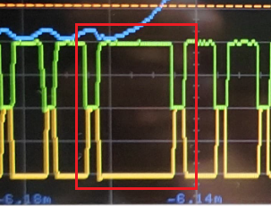
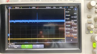
I am facing some uneven glitches in battery charging current. Any timer setting missed ?
I am using "DL_TimerA_setCaptureCompareValue(PWM_0_INST, Duty_Buck, DL_TIMER_CC_2_INDEX);" to modify the PWM duty cycle. Battery charging current is clean if duty cycle is kept constant.
Battery charging current is very clean in case of MSP430.
Regards,
Yogesh

PWM frequency is 100kHz
/* Defines for PWM_0 */
#define PWM_0_INST TIMA0
#define PWM_0_INST_IRQHandler TIMA0_IRQHandler
#define PWM_0_INST_INT_IRQN (TIMA0_INT_IRQn)
#define PWM_0_INST_CLK_FREQ 32000000
/* GPIO defines for channel 2 */
#define GPIO_PWM_0_C2_PORT GPIOA
#define GPIO_PWM_0_C2_PIN DL_GPIO_PIN_10
#define GPIO_PWM_0_C2_IOMUX (IOMUX_PINCM21)
#define GPIO_PWM_0_C2_IOMUX_FUNC IOMUX_PINCM21_PF_TIMA0_CCP2
#define GPIO_PWM_0_C2_IDX DL_TIMER_CC_2_INDEX
/* GPIO defines for channel 2 */
#define GPIO_PWM_0_C2_CMPL_PORT GPIOA
#define GPIO_PWM_0_C2_CMPL_PIN DL_GPIO_PIN_6
#define GPIO_PWM_0_C2_CMPL_IOMUX (IOMUX_PINCM11)
#define GPIO_PWM_0_C2_CMPL_IOMUX_FUNC IOMUX_PINCM11_PF_TIMA0_CCP2_CMPL
/* ##########################################################################################################
* Timer clock configuration to be sourced by / 1 (32000000 Hz)
* timerClkFreq = (timerClkSrc / (timerClkDivRatio * (timerClkPrescale + 1)))
* 32000000 Hz = 32000000 Hz / (1 * (0 + 1))
########################################################################################################## */
static const DL_TimerA_ClockConfig gPWM_0ClockConfig = {
.clockSel = DL_TIMER_CLOCK_BUSCLK,
.divideRatio = DL_TIMER_CLOCK_DIVIDE_1,
.prescale = 0U
};
static const DL_TimerA_PWMConfig gPWM_0Config = {
.pwmMode = DL_TIMER_PWM_MODE_EDGE_ALIGN_UP,
.period = PERIOD_BUCK,
.isTimerWithFourCC = true,
.startTimer = DL_TIMER_STOP,
};
SYSCONFIG_WEAK void SYSCFG_DL_PWM_0_init(void) {
DL_TimerA_setClockConfig(PWM_0_INST, (DL_TimerA_ClockConfig *) &gPWM_0ClockConfig);
DL_TimerA_initPWMMode(PWM_0_INST, (DL_TimerA_PWMConfig *) &gPWM_0Config);
// Set Counter control to the smallest CC index being used
DL_TimerA_setCounterControl(PWM_0_INST,DL_TIMER_CZC_CCCTL2_ZCOND,DL_TIMER_CAC_CCCTL2_ACOND,DL_TIMER_CLC_CCCTL2_LCOND);
DL_TimerA_setCaptureCompareOutCtl(PWM_0_INST, DL_TIMER_CC_OCTL_INIT_VAL_LOW,DL_TIMER_CC_OCTL_INV_OUT_DISABLED,
DL_TIMER_CC_OCTL_SRC_DEAD_BAND,DL_TIMERA_CAPTURE_COMPARE_2_INDEX);
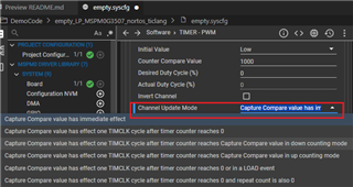
DL_TimerA_setCaptCompUpdateMethod(PWM_0_INST, DL_TIMER_CC_UPDATE_METHOD_IMMEDIATE, DL_TIMERA_CAPTURE_COMPARE_2_INDEX);
DL_TimerA_setCaptureCompareValue(PWM_0_INST, 20, DL_TIMER_CC_2_INDEX);
DL_TimerA_setDeadBand(PWM_0_INST, DEAD_TIME_BUCK, DEAD_TIME_BUCK, DL_TIMER_DEAD_BAND_MODE_0);
DL_TimerA_enableClock(PWM_0_INST);
DL_TimerA_setCCPDirection(PWM_0_INST , DL_TIMER_CC2_OUTPUT );
}
PWM update:
DL_TimerA_setCaptureCompareValue(PWM_0_INST, Duty_Buck, DL_TIMER_CC_2_INDEX);