This thread has been locked.

If you have a related question, please click the "Ask a related question" button in the top right corner. The newly created question will be automatically linked to this question.

AM2432: Review my timing analysis

Part Number: AM2432

Tool/software:

Hi,

Could you kindly review my timing analysis?

We are planning to use the below devices in the upcoming project.
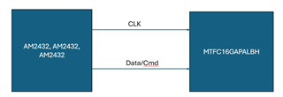
SoC:

Legacy SDR mode:

Tclk(MMC0) = 40ns

Td= Tclk-dV or Tclk-cmd = min(-2.3ns), max(2.9ns)

eMMC : JEDEC Complaint

Tsetup(min) = 3ns

Thold(min) = 3ns

Toutput_delay(min/max)= 2.5ns/13.7ns

Let’s say SoC is driving the clk and command, in that case below will be our timing analysis

Td + Tpcb_data_delay(max)  < Tpcb_clk_delay  + Tclk - Tsetup_emmc ----------------  eq1

Tpcb_data_delay(max)  - Tpcb_clk_delay   < Tclk - Tsetup_emmc – Td

Tpcb_data_delay(max)  - Tpcb_clk_delay < 40- 3-2.9

Tpcb_data_delay(max)  - Tpcb_clk_delay  <  34.1ns

Td  +  Tpcb_data_delay(min) > Thold_emmc  + Tpcb_clk_delay  -------------------------eQ2

Tpcb_data_delay(min) - Tpcb_clk_delay > Thold_emmc   - Td

Tpcb_data_delay(min) - Tpcb_clk_delay >  3-(-2.3)

Tpcb_data_delay(min) - Tpcb_clk_delay >  5.3ns

That means my data or command trace delay should fall between 5.3 ns and 34.1 ns relative to the clock.

Assuming a standard PCB trace delay of 150 ps/inch, achieving a 5.3 ns delay would require routing the trace approximately 35 inches longer than the clock trace — which is clearly impractical.

I feel like I might be missing something here. Could you please help clarify?

Is there any eMMC routing guidelines available with the skew details in any of the TI documentation?

  • You are not including the additional half cycle delay associated with the SOC changing data on the falling edge of clock. See the figure titled "MMC0 – Legacy SDR – Transmit Mode", where it shows the delays are relative to the falling edge of CLK.

    We define the expected PCB trace delays in the datasheet. See the "MMC0 Timing Conditions" table.

    Regards,
    Paul

  • Where in my calculation I have to include that time?

  • The 2.9ns value you used in equation #1 for output delay max should have been [2.9ns + 20ns] = 22.9ns and the -2.3ns value you used in equation #2 for output delay min should have been [(-2.3ns) + 20ns] = 17.7ns. The SOC is changing the DAT and CMD signals on the falling edge of CLK. The SOC data sheet values are defined relative the falling edge of CLK as shown in the switching characteristics timing diagram. The eMMC device setup/hold requirements are relative to the rising edge of CLK. Your original equations assumed the SOC was changing the DAT and CMD signals on the rising edge of CLK, but these signals actual change 20ns later when using a 40ns CLK period. Therefore, you need to effectively add 20ns to the min and max delays in your formulas to account for the additional 1/2 clock period delay.

    Regards,
    Paul

  • Ok, here are my new values. But, I am still not able to get to conclusion since this is far beyond datasheet values.

    Tpcb_data_delay(max)  - Tpcb_clk_delay < 40- 3-22.9

    Tpcb_data_delay(max)  - Tpcb_clk_delay < 14.1

    Tpcb_data_delay(min) - Tpcb_clk_delay >  3-(-2.3+20)

    Tpcb_data_delay(min) - Tpcb_clk_delay > -14.7

  • I forgot to mention you equation #2 is incorrect. The earliest the SOC is changing DAT/CMD after the rising edge of CLK is [(-2.3) + 20ns] = 17.7ns. The eMMC device requires the DAT/CMD signals to remain valid for at least 3ns after the rising edge of CLK. The hold time margin calculation is (17.7ns - 3ns) = 14.7ns. So, the SOC is providing 14.7ns of additional margin over the eMMC device hold time requirement. 

    The latest the SOC is changing DAT/CMD after the rising edge of CLK is [(2.9) + 20ns] = 22.9ns. The eMMC device requires the DAT/CMD to be valid at least 3ns before the rising edge of CLK. The setup time margin calculation is (40ns - 22.9ns -3ns) = 14.1ns, when the period of CLK is 40ns. So, the SOC is providing 14.1ns of margin over the eMMC device setup time requirement.

    The above calculations assume the DAT/CMD PCB trace delays are approximately equal to the CLK PCB trace delay. The setup margin increases, and the hold margin decreases when the CLK PCB trace delay is larger than the DAT/CMD PCB trace delays. The setup margin is decreased, and the hold margin is increased when the CLK PCB trace delay is small than the DAT/CMD PCB trace delays.

    Regards,
    Paul

  • Thank you so much for the explaination.

    I would also like to know, In the mmc0 timing condition table why does td(Trace Delay)(min) is 126ps. How this is calculated?.

  • The min trace delay of 126ps is required to meet a hold time in one of the data transfer modes. It was determined from multiple timing simulations during timing closure of the MMC0 peripheral. This is too complex for me to explain via E2E. Design your PCB to meet the requirements and the peripheral will work as expected for any eMMC compliant device operating in any data transfer mode.