This thread has been locked.

If you have a related question, please click the "Ask a related question" button in the top right corner. The newly created question will be automatically linked to this question.

TMDSEMU110-U: VTREF internal circuity question

Part Number: TMDSEMU110-U

Tool/software:

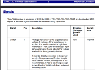
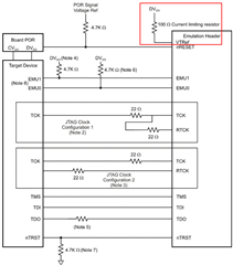
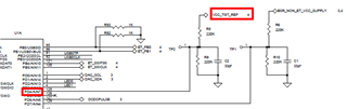
For the CTI-20 pinout, pin 5 VTRef. I found some internal documentation at the company I work for that calls out there is a 100Ω+diode pull down on this pin internal to the device. I can't find any information in the user manual or app note that calls this circuitry out. Wanted to confirm what the internal circuitry for this pin looks like and if there is no pull-down circuit, what is the expected current draw on this pin? 

Thank you for your time. 

  • Hi Josh,

    Do you mean this circuitry is internal to the debugger itself or internal to the MCU/IC implemented in the debugger?

    I am including a quick description of the VTREF pin for reference. When you say internal to the device.

    https://developer.arm.com/documentation/101714/1-0/Debug-and-trace-interface/Target-Voltage-Reference-signals?lang=en

    I am unable to find any details regarding a diode connection here, however, the typical JTAG emulator circuit requires a 100Ω pull up resistor. The signal needs to be pulled up to the voltage source level required by the target device by a current limiting resistor.

    The current draw on this pin is a characteristic of the IC designed into the debugger hardware. I am reaching out to a few other team member to try to find an answer here.

    Best Regards,

    Zackary Fleenor

  • Zackary, thank you for the reply. I am curious about the entire circuit path from the VTREF pin, through the debugger cable, and anything in the debugger itself. We have an external 100Ω pullup resistor on this pin in our design (as recommended), I want to ensure that we have appropriately sized this pullup resistor for the voltage drop and power dissipation it will experience. 

    Thank you for looking into the current draw on this pin, that will be very helpful information. From the description in the first screenshot that calls out VTREF/2, and asks that this pin is pulled up to the IO supply for the processor, and the 100Ω pull up recommended in the second screenshot. Does this imply that there must be a 100Ω pulldown somewhere internal to the debugger to create this voltage division (VTREF/2)? Just trying to piece together where we got this assumption (at my company) for the 100Ω pulldown somewhere in the debugger. 

    Regards,

    -Josh  

  • Hello Josh,

    I did some more digging here. The VTREF/2 signal feeds into a typical ADC channel (AIN7) of the TM4C1294 device. There are already 2x 220kΩ  resistors in the PCB design to create the voltage division by 2 while meeting the criteria described previously of "strong enough to overdrive the 100kΩ pull down resistor of the cable". I am unaware of any other 100Ω pulldown used with the VTREF pin/signal.

    Best Regards,

    Zackary Fleenor

  • Thank you for your help Zackary, this resolves this issue for me.