This thread has been locked.

If you have a related question, please click the "Ask a related question" button in the top right corner. The newly created question will be automatically linked to this question.

AM2612: GPIO_XBAR_INTRTR0

Part Number: AM2612

Tool/software:

Hi,

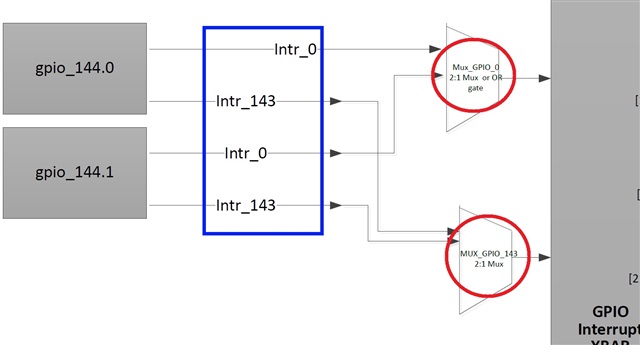
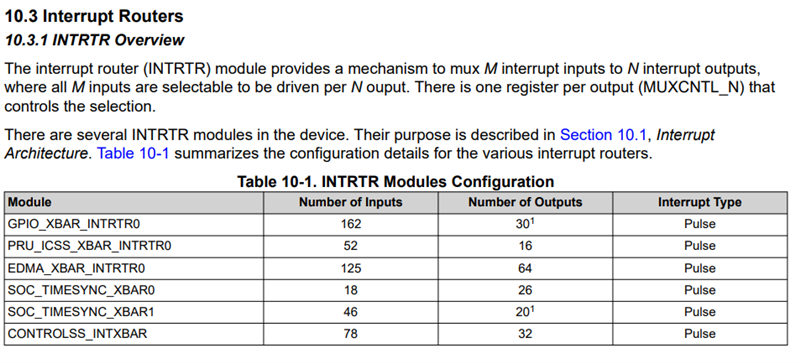
My customer has some questions about "Figure 4-33. GPIO XBAR Interrupt Router Integration Diagram" in the TRM. Could you help to answer their questions below ?


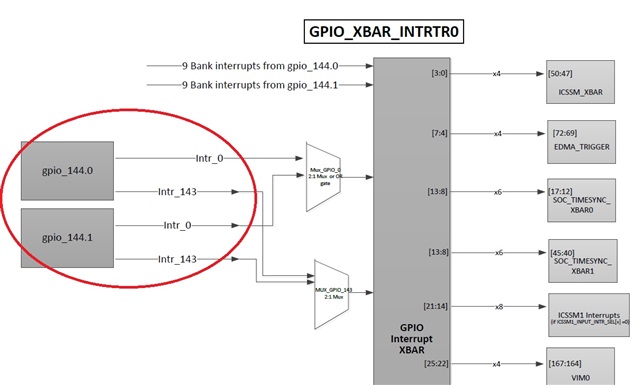
What does “0” of gpio_144.0 mean ?  What does “1” of gpio_144.1 mean ?


The only intr_0 and intr_143 are output from gpio_144.0 or gpio_144_1.

They don’t understand this.

Could you explain this ?

Is there any document which explain this in detail ?


Thanks and regards,

Hideaki

  • Hello,

    Unfortunately the naming in this image is not the most intuitive. gpio_144.0 is referring to the GPIO0 module and gpio_144.1 is referring to the GPIO1 module. 

    Each GPIO module provides up to 144 dedicated general-purpose pins with input and output capabilities separated into 9 banks of 16 pins. There is an interrupt mux for each pin from 0 to 143 (that takes inputs from either GPIO module) and bank level interrupts for each module's banks (18 total).

    Regards,

    Susan

  • Hi Susan,

    Thank you for your reply. Let me confirm a little more.

    Each GPIO module provides up to 144 dedicated general-purpose pins with input and output capabilities separated into 9 banks of 16 pins.

    Could you tell us where any block diagram or description which explains the above is in the TRM or Datasheet ?

    There is an interrupt mux for each pin from 0 to 143 (that takes inputs from either GPIO module)

    This interrupt mux which you mentioned above is the mux red circled in the block diagram below ?

    "each pin from 0 to 143" which you mentioned above is the following blue box ? I don't think so, because the mux is used for only 2 inputs Intr_0 or intr_143.

    We need any other document which explains more detail.

    Thanks and regards,

    Hideaki

  • Hello,

    Unfortunately, I could not immediately find documentation that explains this in more detail, but I reached out to some other team members to see what they know.

    For your other questions:

    Information on the GPIO modules and banks are located in the GPIO chapter of the device TRM.

    As for the interrupt mux (circled in red in your image):

    There are too many inputs to draw out each individual mux, so figure only shows 2 of the 144 muxes for. There are actually a total of 144 muxes. Please see the following section:

    The purpose of the interrupt muxes (again, in red circles) is to separate between the GPIO0 instance (connected to core 0) and GPIO1 instance (connected to core 1). The signal routing inside the blue box in your image is to showcase that the input mux in the red circle will have an input from either GPIO0 or GPIO1 for a given GPIO pin.

    Thank you,

    Susan