This thread has been locked.

If you have a related question, please click the "Ask a related question" button in the top right corner. The newly created question will be automatically linked to this question.

MSPM0G3507: Waiting for an ADC conversion to finish

Part Number: MSPM0G3507

Tool/software:

I have functioning correctly simultaneous ADCs converting on a GPIO trigger, positive edge. All is good.

I write to pin CCK and this starts the conversion.

I want to know when it is finished before I initiate the next conversion....this just hangs:

while(1) {

// Write to GPIO to trigger conversion
DL_GPIO_setPins(GPIO_SA3_CCK_PORT, GPIO_SA3_CCK_PIN);
// Wait to start
while(DL_ADC12_isConversionStarted(ADC12_0_INST)==false)
;
// Wait to finish
while(DL_ADC12_isConversionStarted(ADC12_0_INST)==true)
;
// Toggle 
DL_GPIO_clearPins(GPIO_SA3_CCK_PORT, GPIO_SA3_CCK_PIN);

}

Any clues please ?

  • I didn't find anything in the TRM that says SC toggles (visibly) for a hardware trigger. 

    I would probably poll CPU_INT.RIS.MEMRESIFG0 instead, since that latches the completion without a race.

  • Thanks. Confused.
    Are you saying there is no way of polling if the ADC is currently in the process of doing a conversion (this would include the sample & SAR conversion phase) CPU_INT.RIS.MEMRESIFG0.  --> I do not have interrupts enabled...

  • Hello.

    I tried this:
    // Triggers ADC conversion using an event
    DL_GPIO_setPins(GPIO_SA3_CCK_PORT, GPIO_SA3_CCK_PIN);
    while(DL_ADC12_getRawInterruptStatus(ADC12_0_INST, 0x100) == false);
    ;
    But does not work....it always gets pass the "while" even if I do not trigger an ADC conversion.
    Also I have a had to use 0x100 as CPU_INT.RIS.MEMRESIFG0 is not defined......
    Very confused...
  • My error here...flag already set...cleared it first.

    This seems to work:

    // Trigger ADC conversion

    DL_GPIO_setPins(GPIO_SA3_CCK_PORT, GPIO_SA3_CCK_PIN);

    // Wait for completion

    while(DL_ADC12_getRawInterruptStatus(ADC12_0_INST, ADC12_CPU_INT_IMASK_MEMRESIFG0_MASK ) == false);
       ;
    BUT here I am using DMA to transfer memres0 to a buffer (works fine)...and I think the DMA reading  memres0 is NOT clearing the interrupt flag, which I think it should ??
  • The DMA clears  DMA_TRIG:RIS:MEMRESIFG0 but not CPU_INT:RIS:MEMRESIFG0 [observed behavior]. To use this mechanism you need to clear the former before issuing your CCK trigger (I think that's what you said you're doing?).

    There's also STATUS:BUSY (DL_ADC12_getStatus()) which from the description acts more or less the way you were expecting SC to act. (I haven't tried it.) I expect this would  be susceptible to the same race (stray interrupt between trigger and first getStatus call) as before.

    [Edit: Do you have an ISR for DMA_DONE (i.e. which clears it)? If not, maybe that's the RIS bit you really want to trigger on? I'm not completely clear on the dynamics here.]

  • Hi Bruce, thanks. Getting clearer.

    Attached is what I am trying to do, ADC result DMA to  buffer.

    CK is 750 ns to 1 us.

  • So if your goal is the shortest high period (within constraints) for CK, it seems like the MEMRESIFG is (or STATUS:BUSY) as close as you'll get. I don't see anything in TRM Fig 12-1 that brings the SAMPLE signal [Fig 12-2] outside. (The DMA isn't deterministic in the face of competition from other channels, but I expect it's fast enough.)

    On the Forum, I've seen some hints that the ADC may be sensitive to being triggered while it's BUSY, so if the CK low period is as short as in your example above you probably want to wait for completion (BUSY==0) for that reason.

    Are you still planning to use MISO (or was it MOSI) to do the CK trigger rather than wiggling a GPIO? I'm asking since the former would have a 50% duty but a GPIO (or timer) needn't.

  • Thanks...understood. I now have this:

    // Disable conversions
    DL_ADC12_disableConversions(ADC12_0_INST);
    // Change ADC modes to 8 bit, 50 ns sample time, no averaging
    // ADC 0 - this all works fine
    DL_ADC12_initSingleSample(ADC12_0_INST,
    DL_ADC12_REPEAT_MODE_ENABLED, DL_ADC12_SAMPLING_SOURCE_AUTO, DL_ADC12_TRIG_SRC_EVENT,
    DL_ADC12_SAMP_CONV_RES_8_BIT, DL_ADC12_SAMP_CONV_DATA_FORMAT_UNSIGNED);

    DL_ADC12_setSampleTime0(ADC12_0_INST,2);       //2 = 50 n

    DL_ADC12_configConversionMem(ADC12_0_INST, ADC12_0_ADCMEM_0,
    DL_ADC12_INPUT_CHAN_0, DL_ADC12_REFERENCE_VOLTAGE_EXTREF, DL_ADC12_SAMPLE_TIMER_SOURCE_SCOMP0, DL_ADC12_AVERAGING_MODE_DISABLED,
    DL_ADC12_BURN_OUT_SOURCE_DISABLED, DL_ADC12_TRIGGER_MODE_TRIGGER_NEXT, DL_ADC12_WINDOWS_COMP_MODE_DISABLED);
    DL_ADC12_enableConversions(ADC12_0_INST);
    // Now do a CCK to trigger ADC (GPIO out -> GPIO in -> event trigger, positive edge)
    DL_GPIO_setPins(GPIO_SA3_CCK_PORT, GPIO_SA3_CCK_PIN);
    //There is a latency for conversion start (sample) from CCK positive edge, status is therefore just ref buffer ready high
    while(DL_ADC12_getStatus(ADC12_0_INST)== ADC12_STATUS_REFBUFRDY_READY)
    ;
    // Conversion (sample) must have started, wait for completion of conversion
    while(DL_ADC12_getStatus(ADC12_0_INST)==(ADC12_STATUS_BUSY_ACTIVE | ADC12_STATUS_REFBUFRDY_READY))
    ;
    // CCK low
    DL_GPIO_clearPins(GPIO_SA3_CCK_PORT, GPIO_SA3_CCK_PIN);
    I would expect as I change the sample time, the pulse width of my CCK would change....it does not...puzzling !
  • Bug in my code, Vref buffer not used...

    However, If I now do this, it just hangs and never exists the loop ??

    // Now do a CCK to trigger ADC (GPIO out -> GPIO in -> event trigger, positive edge)
    DL_GPIO_setPins(GPIO_SA3_CCK_PORT, GPIO_SA3_CCK_PIN);
    //There is a latency for conversion start (sample) from CCK positive edge
    DL_GPIO_setPins(GPIO_SA3_CCK_PORT, GPIO_SA3_CCK_PIN);

    while(DL_ADC12_getStatus(ADC12_0_INST)== ADC12_STATUS_BUSY_IDLE)
          ;
    while(DL_ADC12_getStatus(ADC12_0_INST)==(ADC12_STATUS_BUSY_ACTIVE))
          ;
  • Which loop gets stuck? (As I said, I haven't tried STATUS:BUSY; I suppose it works as advertised.)

    Is there a reason for setting the CCK pin (high) twice?

  • First loop...

    "Is there a reason for setting the CCK pin (high) twice?"

    it's Monday....

    This works for the first CCK

    DL_GPIO_setPins(GPIO_SA3_CCK_PORT, GPIO_SA3_CCK_PIN);

    while(DL_ADC12_getRawInterruptStatus(ADC12_0_INST, ADC12_DMA_TRIG_IMASK_MEMRESIFG0_SET) == false)
         ;
    But not for subsequentCCK  because I guess the bit needs to be reset....but does not the DMA reset this on a read ???
  • When you asked about it before, I did an experiment (a slightly-hacked version of adc12_max_freq_dma) that convinced me that the DMA clears DMA_TRIG.RIS.MEMRESIFG0 but not CPU_INT.RIS.MEMRESIFG0.

    The DMA read (of MEMRES0) itself apparently doesn't count as a "read" in TRM Table 12-20, rather it's the DMA-ACK that clears the RIS bit, and clearing CPU_INT.RIS.MEMRESIFG0 requires a read from the CPU. TRM Sections 12.2.14.1 and 12.2.14.3 hint at this distinction, though the former doesn't explicitly mention the MEMRES registers.

    DL_ADC12_clearInterruptStatus() refers to CPU_INT. The corresponding call for DMA_TRIG is DL_ADC12_clearDMATriggerStatus().

    Are you seeing different behavior?

  • Hello...yes I think so, sort of..

    // Now do a CCK to trigger ADC (GPIO out -> GPIO in -> event trigger, positive edge)
    DL_GPIO_setPins(GPIO_SA3_CCK_PORT, GPIO_SA3_CCK_PIN);
    convert=0;
    // Wait for conversion end via DMA handshake, count time with a pseudo variable, "convert"
    while(DL_ADC12_getRawInterruptStatus(ADC12_0_INST, ADC12_DMA_TRIG_RIS_MEMRESIFG0_MASK) == false)
        convert++;
    // CCK low
    DL_GPIO_clearPins(GPIO_SA3_CCK_PORT, GPIO_SA3_CCK_PIN);
    // Now do remaining 64 CCKS
    #pragma GCC unroll 64
    for(i=0;i<64;i++){
    convert=0;
    DL_GPIO_setPins(GPIO_SA3_CCK_PORT, GPIO_SA3_CCK_PIN);
    while(DL_ADC12_getRawInterruptStatus(ADC12_0_INST, ADC12_DMA_TRIG_RIS_MEMRESIFG0_MASK) == false)
            convert++;
    DL_GPIO_clearPins(GPIO_SA3_CCK_PORT, GPIO_SA3_CCK_PIN);
    }
    // Done
    The first CCK, before the for-loop, I get convert=7....consistent with the large sample time I have used.
    If I set a break before the for-loop  I can see ADC12_DMA_TRIG_RIS_MEMRESIFG0 is set to zero.
    BUT in the for-loop convert is always zero, suggesting RIS is always set ????
    And I see this in my CCK....changing sample time, changes width of first CCK.
  • Before each

    DL_GPIO_setPins(GPIO_SA3_CCK_PORT, GPIO_SA3_CCK_PIN);

    insert

    > DL_ADC12_clearInterruptStatus(ADC12_0_INST, ADC12_DMA_TRIG_RIS_MEMRESIFG0_MASK); // Clear stale

    Since the DMA isn't doing it (that's actually an advantage in this case) you have to.

  • Thanks, but should not the DMA clear this  each time it does a transfer ?

    8.2.5.4 Hardware Event Handling

    In the case of an event which sources a DMA trigger (DMA_TRIG) or a generic event (GEN_EVENT), the IIDX

    register is not used. A four-way event handshake is performed between the peripheral generating the event

    and the hardware entity which is subscribed to the event (for example, the DMA or a secondary peripheral).

    The four-way event handshake will clear the corresponding interrupt status bits in the RIS and MIS registers

    automatically.

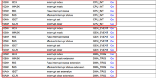
  • There are 3x different RIS registers. If you breakpoint at the second setPins call, I expect you'll see that DMA_TRIG.RIS has MEMRESIFG0=0, but CPU_INT.RIS has MEMRESIFG0=1. This is also consistent with your code's behavior.

  • Hi…sorry I am being dumb, I use dma ris in the loop so why does the dma not clear it the trm above says it dies ???

  • The definition for DL_ADC12_getRawInterruptStatus looks like:

    __STATIC_INLINE uint32_t DL_ADC12_getRawInterruptStatus(
        const ADC12_Regs *adc12, uint32_t interruptMask)
    {
        return (adc12->ULLMEM.CPU_INT.RIS & interruptMask);
    }

    i.e. it looks only at CPU_INT.RIS. By contrast you get to DMA_TRIG.RIS with:

    __STATIC_INLINE uint32_t DL_ADC12_getRawDMATriggerStatus(
        const ADC12_Regs *adc12, uint32_t dmaMask)
    {
        return (adc12->ULLMEM.DMA_TRIG.RIS & ~(dmaMask));
    }
     

    [That "~" sure doesn't look right, does it? I wonder if anyone has ever used this function.]

    In practice, the RIS bit definitions for the (multiple) RIS registers in each peripheral are the same (also IMASK/ICLR/etc), but named differently (CMSIS requirement), so (ADC12_DMA_TRIG_RIS_MEMRESIFG0_MASK == ADC12_CPU_INT_RIS_MEMRESIFG0_MASK); using an alternate bit name doesn't reference a different RIS register.

    [Edit: In my suggested code above, I didn't notice that you were using the DMA_TRIG_RIS definition -- I just copied what you had. But it would still work.]

  • Hi, thanks.

    I think I am going to have to do this all a different way.

    Despite your (excellent) efforts I simply do not understand why I have to:

    Before each

    > DL_GPIO_setPins(GPIO_SA3_CCK_PORT, GPIO_SA3_CCK_PIN);

    insert

    > DL_ADC12_clearInterruptStatus(ADC12_0_INST, ADC12_DMA_TRIG_RIS_MEMRESIFG0_MASK); // Clear stale

    Since the DMA isn't doing it (that's actually an advantage in this case) you have to.

    Because the TRM says the RIS bit resets after each DMA, so why do I need to clear it ???

    8.2.5.4 Hardware Event Handling

    In the case of an event which sources a DMA trigger (DMA_TRIG) or a generic event (GEN_EVENT), the IIDX

    register is not used. A four-way event handshake is performed between the peripheral generating the event

    and the hardware entity which is subscribed to the event (for example, the DMA or a secondary peripheral).

    The four-way event handshake will clear the corresponding interrupt status bits in the RIS and MIS registers

    automatically.

  • "the RIS bit resets after each DMA". The key is: Which RIS[:MEMRESIFG0] bit? There are 3x RIS:MEMRESIFG0 bits in the ADC. Observed behavior is that the DMA only clears 1x of them, and that one is not the one you're looking at. (If it were clearing all 3x, it would happen too fast for your loop to see it high and your code would have acted differently.)

    What behavior did you see when you inserted the DL_ADC12_clearInterruptStatus() call I suggested above? 

    Unsolicited: Is what you're writing a one-shot experiment or the way you intend to do the triggering long-term? The STATUS:BUSY check will probably work 99% of the time [assuming not 0%] and so might suffice for an experiment.

  • Today I had a chance to try STATUS:BUSY, and I think it doesn't do what you want. TRM Sec 12.2.13 says "For repeat single conversion, it signals that repeat single operation has begun and has not ended." and based on observed behavior I think that needs to be read literally. The mode is "repeat single" -- not "single" with repeat-ability -- and it starts (goes BUSY) with the first trigger and ends Never (unless you toggle ENC).

    This is also consistent with the results of your earlier experiment.

  • Hi Filip,

    Regarding your question on DMA, I want to jump in and add some comments.

    M0 supports three different EVENT system, the CPU_INT is used for CPU interrupt request.

    The second is GEN EVENT, which used for peripheral trigger, such as GPIO trigger ADC by event system.

    The last one is DMA EVNT, so that DMA will clear this by hardware if DMA transfer happens.

    As for ADC conversion status monitor, normally you are polling the CPU_INT RIS, and then you should clear the CPU_INT RIS, as it will not be cleared by DMA.

    B.R.

    Sal

  • Thanks.

    This seems to work:

    // Clear interrupt memres0

    DL_ADC12_clearInterruptStatus(ADC12_0_INST, ADC12_CPU_INT_IMASK_MEMRESIFG0_MASK);

    // 64 clocks
    #pragma GCC unroll 64

    for(i=0;i<64;i++){
    // CCK high, trigger ADC via event
    DL_GPIO_setPins(GPIO_SA3_CCK_PORT, GPIO_SA3_CCK_PIN);
    // Wait for memres0
    while(DL_ADC12_getRawInterruptStatus(ADC12_0_INST, ADC12_CPU_INT_IMASK_MEMRESIFG0_MASK) == false)
                     ;
    // CCK low
    DL_GPIO_clearPins(GPIO_SA3_CCK_PORT, GPIO_SA3_CCK_PIN);
    // Clear interrupt memres0
    DL_ADC12_clearInterruptStatus(ADC12_0_INST, ADC12_CPU_INT_IMASK_MEMRESIFG0_MASK);
    NOP_10; // Ten NOP delay
    } // end for
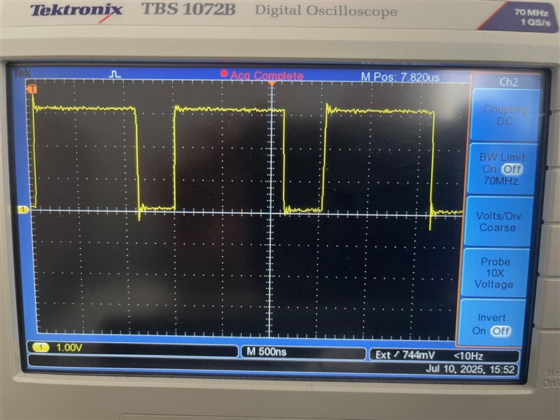
    BUT..when I look at CCK on a 'scope, hard to understand why CCK is high for over a microsecond ?
    DL_ADC12_setSampleTime0(ADC12_1_INST,15); //2 = 50 ns
    is good, I can modulate CCK high by changing above.

    8.1.5 Event Propagation Latency 

    Generic route channels implement a four-way hardware handshake between the publishing entity and the

    subscribing entity. This handshake requires four ULPCLK cycles to complete:

    In my case ULPCLK is 25 ns, so above is 100 ns.
    Sample time time is 375 ns from above also.
    I also have this case:

    (C) When ADCCLK is sourced from ULPCLK, the synchronization delay (tsync) is bypassed and the SAMPLE signal gets asserted with the ADC Trigge

    And nine clock cycles for ADC 8 bit conversion including write to memres0.

    So I think all that takes; 100ns + 300ns + 9*25ns = 625 ns

    And then take CCK low....

    Seems to be a large discrepancy..

  • All I can think of is that the DMA is interfering with the CPU bus (polling) activity. Reading TRM Chapter 5 it's never been clear to me whether the CPU or DMA gets priority for bus activity (and at what granularity).

    A quick (maybe) experiment might be to remove the line of code that enables the DMA channel (the DMA requests and data just get lost) and see if your waveform changes.