This thread has been locked.

If you have a related question, please click the "Ask a related question" button in the top right corner. The newly created question will be automatically linked to this question.

TMDSEMU110-U: Is it possible to debug without entering VTREF in the IDE settings?

Expert 2670 points
Part Number: TMDSEMU110-U
Other Parts Discussed in Thread: CC2651R3SIPA

Tool/software:

Hi All,

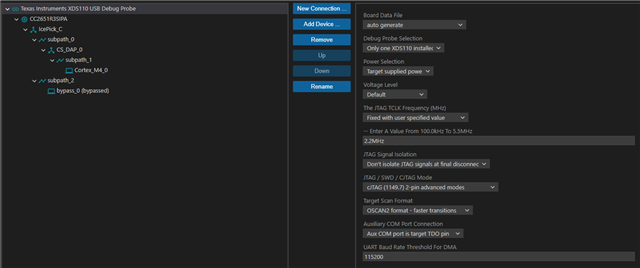
When debugging CC2651R3SIPA using TMDSEMU110-U,
I understand that the power supply voltage of CC2651R3SIPA must be input to the ‘VTREF’ terminal on the TMDSEMVU110-U side.
Is this correct?
Or is it possible to debug without inputting to VTREF in the IDE settings?

Best Regards,

Ito

  • Hi Ite,

    Let me loop you into the HW team to comment on this.

    Best Regards,

    Jan

  • Hi Jan,

    Thank you for your help,

    Best Regards,

    Ito

  • Hi,

    I understand that the power supply voltage of CC2651R3SIPA must be input to the ‘VTREF’ terminal on the TMDSEMVU110-U side.
    Is this correct?

    If I understood your question correctly, the VDDS net of the CC2651R3SIPA must be connected to the TVRef (or VTRef) pin of the TMDSEMU110-U JTAG connector. However, the JTAG/SWD specification states that this pin is a sense pin to detect if there is voltage present on the device  and is not designed to provide power to the device. Moreover, in the TMDSEMU110-U design, the TVRef pin will also power the I/O voltage translators, so the JTAG/SWD signal matches the power supply of the target. 

    Our Launchpad designs use this pin as a supply voltage pin, which is done for convenience for the development kit but it deviates from the JTAG standards. 

    Or is it possible to debug without inputting to VTREF in the IDE settings?

    This option is masked if you select "Target Supplied Power" in the Target Configuration settings

    Regards,

    Rafael

  • Hi Rafael,

    Thank you for your reply.

    This option is masked if you select "Target Supplied Power" in the Target Configuration settings

    Does this mean that debugging and FW changes are possible without applying voltage to the ‘VTREF’ terminal on the TMDSEMU110-U side?

    TMDSEMU110-U and CC2651R3SIPA are designed for access via two lines, TDI and TDO. Is there any problem with this design?

    Best Regards,

    Ito

  • Hi Rafael,

    Can you answer this question?

    Best Regards,

    Ito

  • Hi Rafael,

    Can you answer this question?

    Best Regards,

    Ito

  • Ito,

    Please apologize for the delay; I have been sidetracked in the past two weeks.

    Does this mean that debugging and FW changes are possible without applying voltage to the ‘VTREF’ terminal on the TMDSEMU110-U side?

    No. The debug probe TMDSEMU110-U must have VDDS tied to the VTRef pin in order to properly detect voltage on the target device. Failing to do so would trigger error 267 as shown in the Debugging JTAG page below:

    https://software-dl.ti.com/ccs/esd/documents/ccs_debugging_jtag_connectivity_issues.html

    TMDSEMU110-U and CC2651R3SIPA are designed for access via two lines, TDI and TDO. Is there any problem with this design?

    Not at all. The CC2651R3SIPA can operate in 4-wire JTAG or 2-wire cJTAG. The 4-wire JTAG requires TDI/TDO/TRST/TMS (plus reset to properly flash the device). The operation in 2-wire cJTAG has no functional limitations for this class of device when compared to 4-wire JTAG and has the advantage of using only two wires.  

    Hope this helps,

    Rafael