A related question is a question created from another question. When the related question is created, it will be automatically linked to the original question.
If you have a related question, please click the "Ask a related question" button in the top right corner. The newly created question will be automatically linked to this question.
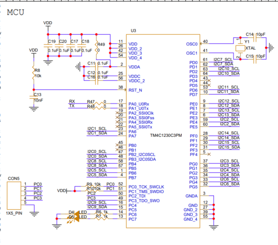
- I don't see enough LDO filter cap on VDDC. The recommendation is 3.3uF to 3.4uF. I only see 0.3uF on your schematic.
- Is there a bulk capacitance on VDD? I only see 0.1uF decoupling cap on each VDD pin. The combined VDD and VDDA bulk capacitance of the microcontroller is typically between 2 μF and 22 μF. Perhaps you have these on a different schematic page.
- The recommendation is to have pullup resistor on TCK/TMS/TDI if the JTAG signals are far from the MCU as it may pick noises. Otherwise, the MCU has internal pullup already.