Other Parts Discussed in Thread: UNIFLASH, , SYSCONFIG
Tool/software:
Hi All,
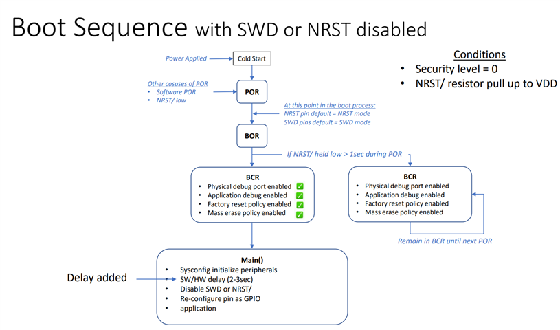
I'm using MSPM0C1104SDDFR SoT23-8 8 pin microcontroller . I upon referring the reference manual of the MSPMC1104 IC I understood that i can disable SWD pins in software and access them as a GPIO Pin, and can can enable them only by POR (Power on Reset ) .
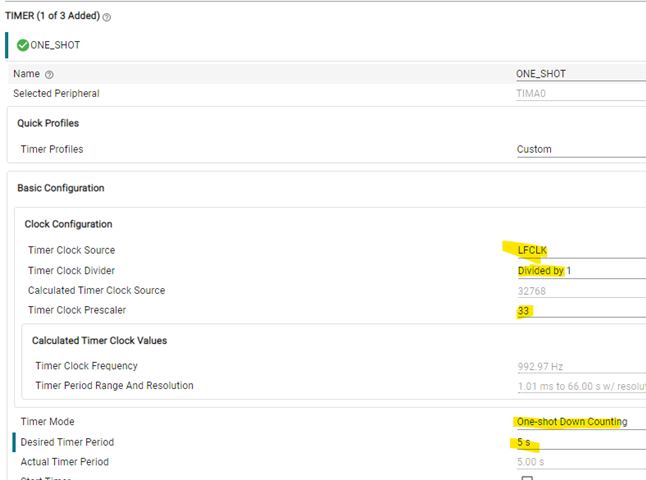
In my code i Disabled the SWD pins using the API " DL_SYSCTL_disableSWD();" with delay cycles 10000000 "delay_cycles(10000000);" assuming it as 10 sec . After this is configered those pins as a PWM pin by the following api's
" DL_GPIO_initPeripheralOutputFunction(IOMUX_PINCM21,IOMUX_PINCM21_PF_TIMA0_CCP0);
DL_GPIO_enableOutput(GPIOA, DL_GPIO_PIN_20);
DL_GPIO_initPeripheralOutputFunction(IOMUX_PINCM20,IOMUX_PINCM20_PF_TIMA0_CCP2);
DL_GPIO_enableOutput(GPIOA, DL_GPIO_PIN_19);
DL_GPIO_setDigitalInternalResistor(IOMUX_PINCM21, (IOMUX_PINCM_PIPU_DISABLE | IOMUX_PINCM_PIPD_DISABLE));
DL_GPIO_setDigitalInternalResistor(IOMUX_PINCM20, (IOMUX_PINCM_PIPU_DISABLE | IOMUX_PINCM_PIPD_DISABLE));
DL_TimerA_setCCPDirection(TIMA0 , DL_TIMER_CC0_OUTPUT | DL_TIMER_CC2_OUTPUT ); "
I flashed the 8pin microcontroller in my custom board i waited for 10 sec No pulse where produced from the PWM pin (previously SWD Pins) . I already checked this program of PWM with MSPMC11041 launch pad ( except the SWD pin change to GPIO).
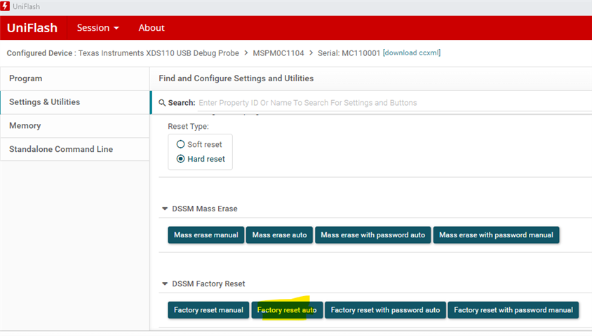
Since No pulse produced from my 8 pin microcontroller . I tried to flash it again by proceeding with the POR ( by removing and plugging the 4pin of microcontroller from 3.3V source which holding the RESET for more than 5 sec) but i can't able to flash the microcontroller from then on. Plz point out my mistakes and help me out .
my requirement is that I wanted to disable the SWD pin and use that pin as PWM pins . after POR i want the SWD to be enabled for 5 to 10 sec .
/*
 * Copyright (c) 2021, Texas Instruments Incorporated
 * All rights reserved.
 *
 * Redistribution and use in source and binary forms, with or without
 * modification, are permitted provided that the following conditions
 * are met:
 *
 * *  Redistributions of source code must retain the above copyright
 *    notice, this list of conditions and the following disclaimer.
 *
 * *  Redistributions in binary form must reproduce the above copyright
 *    notice, this list of conditions and the following disclaimer in the
 *    documentation and/or other materials provided with the distribution.
 *
 * *  Neither the name of Texas Instruments Incorporated nor the names of
 *    its contributors may be used to endorse or promote products derived
 *    from this software without specific prior written permission.
 *
 * THIS SOFTWARE IS PROVIDED BY THE COPYRIGHT HOLDERS AND CONTRIBUTORS "AS IS"
 * AND ANY EXPRESS OR IMPLIED WARRANTIES, INCLUDING, BUT NOT LIMITED TO,
 * THE IMPLIED WARRANTIES OF MERCHANTABILITY AND FITNESS FOR A PARTICULAR
 * PURPOSE ARE DISCLAIMED. IN NO EVENT SHALL THE COPYRIGHT OWNER OR
 * CONTRIBUTORS BE LIABLE FOR ANY DIRECT, INDIRECT, INCIDENTAL, SPECIAL,
 * EXEMPLARY, OR CONSEQUENTIAL DAMAGES (INCLUDING, BUT NOT LIMITED TO,
 * PROCUREMENT OF SUBSTITUTE GOODS OR SERVICES; LOSS OF USE, DATA, OR PROFITS;
 * OR BUSINESS INTERRUPTION) HOWEVER CAUSED AND ON ANY THEORY OF LIABILITY,
 * WHETHER IN CONTRACT, STRICT LIABILITY, OR TORT (INCLUDING NEGLIGENCE OR
 * OTHERWISE) ARISING IN ANY WAY OUT OF THE USE OF THIS SOFTWARE,
 * EVEN IF ADVISED OF THE POSSIBILITY OF SUCH DAMAGE.
 */

#include <ti/driverlib/m0p/dl_interrupt.h>
#include "ti_msp_dl_config.h"

bool pulseTerminal=0 ;


int main(void)
{

    SYSCFG_DL_init();


    for(uint32_t i=0 ; i<100 ;i++)
     delay_cycles(10000000);
    DL_SYSCTL_disableSWD();

  DL_GPIO_initPeripheralOutputFunction(IOMUX_PINCM21,IOMUX_PINCM21_PF_TIMA0_CCP0);
  DL_GPIO_enableOutput(GPIOA, DL_GPIO_PIN_20);
  DL_GPIO_initPeripheralOutputFunction(IOMUX_PINCM20,IOMUX_PINCM20_PF_TIMA0_CCP2);
  DL_GPIO_enableOutput(GPIOA, DL_GPIO_PIN_19);

	DL_GPIO_setDigitalInternalResistor(IOMUX_PINCM21,  (IOMUX_PINCM_PIPU_DISABLE | IOMUX_PINCM_PIPD_DISABLE));
	DL_GPIO_setDigitalInternalResistor(IOMUX_PINCM20,   (IOMUX_PINCM_PIPU_DISABLE | IOMUX_PINCM_PIPD_DISABLE));
   DL_TimerA_setCCPDirection(TIMA0 , DL_TIMER_CC0_OUTPUT | DL_TIMER_CC2_OUTPUT );
    NVIC_EnableIRQ(TIMA0_INT_IRQn);

    DL_Timer_startCounter(TIMA0);


    while (1)
    {

    }
}


void TIMA0_IRQHandler(void)
{
  pulseTerminal =! pulseTerminal;
  if(pulseTerminal)
   DL_Timer_setCCPOutputDisabledAdv(TIMA0, DL_TIMER_CCP0_DIS_OUT_ADV_SET_BY_OCTL| DL_TIMER_CCP1_DIS_OUT_ADV_FORCE_LOW| \
                                        DL_TIMER_CCP2_DIS_OUT_ADV_FORCE_LOW | DL_TIMER_CCP3_DIS_OUT_ADV_FORCE_LOW);
  else
  {
    DL_Timer_setCCPOutputDisabledAdv(TIMA0, DL_TIMER_CCP0_DIS_OUT_ADV_FORCE_LOW| DL_TIMER_CCP1_DIS_OUT_ADV_FORCE_LOW| \
                                          DL_TIMER_CCP2_DIS_OUT_ADV_SET_BY_OCTL | DL_TIMER_CCP3_DIS_OUT_ADV_FORCE_LOW);
  }


}