This thread has been locked.

If you have a related question, please click the "Ask a related question" button in the top right corner. The newly created question will be automatically linked to this question.

AM263P4: MCAN baudrate wrong when booting from flash

Part Number: AM263P4
Other Parts Discussed in Thread: SYSCONFIG

Tool/software:

Hi,

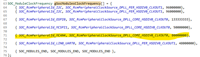
I have a working multicore project that, when I load it with CCS in devboot mode, works just fine. MCAN baudrate is and should be 1000 kbit/s.

However, when this project gets loaded from flash via SBL in OSPI boot mode, the baudrate is wrong with about 310 kbit/s.

  1. What could be the problem here? 
  2. When loading with CCS the GEL-files do a lot of clock configurations. Where/When does this happen when booting via SBL? Do I have to do some additional config in my SBL?

Additional info:

SOC: AM263P4_ZCZ_F
MCAN code mostly from 'mcan_external_read_write' example
SBL code mostly from 'sbl_ospi' example

Best regards,
Frank

  • Hi Frank,

    The clock of MCAN module is configured by Module_clockSetFrequency() in ti_power_clock_config.c. The clock is defined in gSocModulesClockFrequency[] in the same file.

    If it is not configured, the default MCNA clock source is WUCPUCLK (25MHz), and the clock divider is 1.

    If the MCAN clock defined SocModulesClockFrequency[] is 80MHz, the 310Kbps baudrate is expected: 1000kbps * 80MHz/25MHz = 310kbps.

  • so what am I supposed to do now, to solve this?

    MCAN in application code is configured in ti_power_clock_config.c like in your image, and since this is a auto generated file, I cannot change it anyway. Also, adding MCAN to the SBL, does not change the observed behaviour. To me it feels like the SBL does some SOC configuration that is different from the GEL files. 

  • Hi Frank,

    The ROM bootloader configures the core PLL only which are required during boot. The SBL reconfigures the core PLL and Peripheral PLL. The Core CLKOUT0 is 400MHz, and CLKOUT1 is 500MHz, the Per CLKOUT0 is 160MHz, and CLKOUT1 is 192MHz.

    If the MCAN is enabled (sysconfig), the MCAN clock is configured as 80MHz from CORE CLKOUT0. What is the MCAN clock config in your setup (power_clock_config.c)? 

    Please double check the PLL settings (the registers are located at 0x5320_04xx).

  • The clock setup in application code on R5_0 looks like this:

    SOC_ModuleClockFrequency gSocModulesClockFrequency[] = {
        { SOC_RcmPeripheralId_I2C, SOC_RcmPeripheralClockSource_DPLL_PER_HSDIV0_CLKOUT1, 96000000},
        { SOC_RcmPeripheralId_MCAN1, SOC_RcmPeripheralClockSource_DPLL_CORE_HSDIV0_CLKOUT0, 80000000},
        { SOC_RcmPeripheralId_MCAN0, SOC_RcmPeripheralClockSource_DPLL_CORE_HSDIV0_CLKOUT0, 80000000},
        { SOC_RcmPeripheralId_OSPI0, SOC_RcmPeripheralClockSource_DPLL_CORE_HSDIV0_CLKOUT0, 133333333},
        { SOC_RcmPeripheralId_WDT0, SOC_RcmPeripheralClockSource_SYS_CLK, 200000000},
        { SOC_RcmPeripheralId_LIN0_UART0, SOC_RcmPeripheralClockSource_DPLL_PER_HSDIV0_CLKOUT1, 48000000},
        { SOC_MODULES_END, SOC_MODULES_END, SOC_MODULES_END },
    };

    Please answer me the following question for my understanding of the basic workflow:

    • If I use MCAN or LIN or whatever module in application code, do I need to do something additional in the SBL code/sysconfig? Or is it sufficient to do the configuration with sysconfig in the application and the SBL is universal and independent from the application code.

    I already compared the PLL registers. The only difference (CCS vs. OSPI_SBL loading) was the PLL_CORE_CLKCTRL_CLKDCOLDOEN bit in TOP_RCM_PLL_CORE_CLKCTRL and TOP_RCM_PLL_PER_CLKCTRL and some status bits, I think PLL_CORE_STATUS_CLKDCOLDOACK. I can check again tomorrow.

  • If you use OSPI SBL, you need to check the SBL code to make sure the PLL has been reconfigured.

  • I don’t understand what I’m supposed to do.

    Do I need to do something application specific in the SBL or not?

  • The TI OSPI SBL example reconfigures the Core PLL and Peripheral PLL. The Core CLKOUT0 is 400MHz, and CLKOUT1 is 500MHz, the Per CLKOUT0 is 160MHz, and CLKOUT1 is 192MHz.

    SOC_RcmPeripheralClockSource_DPLL_CORE_HSDIV0_CLKOUT0 is used in your setup for MCAN0 and MCAN1, the divider should be 400MHz/80MHz = 5. Can you check if the MCAN divider register is programmed with a right divider?

    MSS_RCM_MCAN0_CLK_SRC_SEL at 0x53208100

    MSS_RCM_MCAN0_CLK_DIV_VAL at 0x53208300

  • Here are all the registers from MMS_CTRL, MMS_RCM and TOP_RCM that are different:

    so the registers you mentioned are identical.

    Address		CCS devboot	SBL OSPI	Register
    			MCAN 1MBd	MCAN 310kBd
    0x50D00020	0x00000000	0x07000700	MSS_CTRL_R5SS0_CONTROL
    0x50D00040	0x00000000	0x00000707	MSS_CTRL_R5SS1_CONTROL
    0x50D0004C	0x00000000	0x00000100	MSS_CTRL_R5SS1_STATUS_REG
    0x50D00054	0x00000000	0x00000011	MSS_CTRL_R5SS1_CORE1_STAT
    0x50D00080	0x00000007	0x00000707	MSS_CTRL_R5SS0_ROM_ECLIPSE
    0x50D00244	0x0000003F	0x00000000	MSS_CTRL_L2IOCRAM_MEM_INIT_DONE
    0x50D00830	0x00000000	0x000001FD	MSS_CTRL_TPCC0_INTAGG_MASK
    0x50D00838	0x00000000	0x00000003	MSS_CTRL_TPCC0_INTAGG_STATUS_RAW
    0x50D18104	0x00000000	0x00000007	MSS_CTRL_R5SS0_CORE0_TCM_ADDRPARITY_ERRAGG_STATUS
    0x50D18108	0x00000000	0x00000007	MSS_CTRL_R5SS0_CORE0_TCM_ADDRPARITY_ERRAGG_STATUS_RAW
    0x50D18164	0x00000000	0x000002D1	MSS_CTRL_R5SS1_CORE0_ADDRPARITY_ERR_ATCM
    0x53208010	0x00000783	0x00000603	MSS_RCM_R5SS0_RST_STATUS
    0x53208024	0x00000707	0x07070007	MSS_RCM_R5SS0_RST_WFICHECK
    0x53208030	0x00000603	0x00000003	MSS_RCM_R5SS1_RST_STATUS
    0x53208044	0x00000707	0x07070707	MSS_RCM_R5SS1_RST_WFICHECK
    0x53208104	0x00000444	0x00000000	MSS_RCM_MCAN1_CLK_SRC_SEL
    0x53208108	0x00000444	0x00000000	MSS_RCM_MCAN2_CLK_SRC_SEL
    0x5320810C	0x00000444	0x00000000	MSS_RCM_MCAN3_CLK_SRC_SEL
    0x5320811C	0x00000222	0x00000000	MSS_RCM_RTI2_CLK_SRC_SEL
    0x53208120	0x00000222	0x00000000	MSS_RCM_RTI3_CLK_SRC_SEL
    0x53208130	0x00000222	0x00000000	MSS_RCM_WDT2_CLK_SRC_SEL
    0x53208134	0x00000222	0x00000000	MSS_RCM_WDT3_CLK_SRC_SEL
    0x5320813C	0x00000333	0x00000000	MSS_RCM_MCSPI0_CLK_SRC_SEL
    0x53208140	0x00000333	0x00000000	MSS_RCM_MCSPI1_CLK_SRC_SEL
    0x53208144	0x00000333	0x00000000	MSS_RCM_MCSPI2_CLK_SRC_SEL
    0x53208148	0x00000333	0x00000000	MSS_RCM_MCSPI3_CLK_SRC_SEL
    0x5320814C	0x00000333	0x00000000	MSS_RCM_MCSPI4_CLK_SRC_SEL
    0x53208150	0x00000333	0x00000000	MSS_RCM_MMC0_CLK_SRC_SEL
    0x53208158	0x00000333	0x00000000	MSS_RCM_CPTS_CLK_SRC_SEL
    0x53208160	0x00000222	0x00000000	MSS_RCM_CONTROLSS_PLL_CLK_SRC_SEL
    0x53208178	0x00000777	0x00000000	MSS_RCM_LIN1_UART1_CLK_SRC_SEL
    0x5320817C	0x00000777	0x00000000	MSS_RCM_LIN2_UART2_CLK_SRC_SEL
    0x53208180	0x00000777	0x00000000	MSS_RCM_LIN3_UART3_CLK_SRC_SEL
    0x53208184	0x00000777	0x00000000	MSS_RCM_LIN4_UART4_CLK_SRC_SEL
    0x53208188	0x00000777	0x00000000	MSS_RCM_LIN5_UART5_CLK_SRC_SEL
    0x53208204	0x00000444	0x00000000	MSS_RCM_MCAN1_CLK_DIV_VAL
    0x53208208	0x00000444	0x00000000	MSS_RCM_MCAN2_CLK_DIV_VAL
    0x5320820C	0x00000444	0x00000000	MSS_RCM_MCAN3_CLK_DIV_VAL
    0x5320823C	0x00000333	0x00000000	MSS_RCM_MCSPI0_CLK_DIV_VAL
    0x53208240	0x00000333	0x00000000	MSS_RCM_MCSPI1_CLK_DIV_VAL
    0x53208244	0x00000333	0x00000000	MSS_RCM_MCSPI2_CLK_DIV_VAL
    0x53208248	0x00000333	0x00000000	MSS_RCM_MCSPI3_CLK_DIV_VAL
    0x5320824C	0x00000333	0x00000000	MSS_RCM_MCSPI4_CLK_DIV_VAL
    0x53208250	0x00000333	0x00000000	MSS_RCM_MMC0_CLK_DIV_VAL
    0x53208258	0x00000111	0x00000000	MSS_RCM_CPTS_CLK_DIV_VAL
    0x53208404	0x00000410	0x00000001	MSS_RCM_MCAN1_CLK_STATUS
    0x53208408	0x00000410	0x00000001	MSS_RCM_MCAN2_CLK_STATUS
    0x5320840C	0x00000410	0x00000001	MSS_RCM_MCAN3_CLK_STATUS
    0x5320841C	0x00000004	0x00000001	MSS_RCM_RTI2_CLK_STATUS
    0x53208420	0x00000004	0x00000001	MSS_RCM_RTI3_CLK_STATUS
    0x53208430	0x00000004	0x00000001	MSS_RCM_WDT2_CLK_STATUS
    0x53208434	0x00000004	0x00000001	MSS_RCM_WDT3_CLK_STATUS
    0x5320843C	0x00000308	0x00000001	MSS_RCM_MCSPI0_CLK_STATUS
    0x53208440	0x00000308	0x00000001	MSS_RCM_MCSPI1_CLK_STATUS
    0x53208444	0x00000308	0x00000001	MSS_RCM_MCSPI2_CLK_STATUS
    0x53208448	0x00000308	0x00000001	MSS_RCM_MCSPI3_CLK_STATUS
    0x5320844C	0x00000308	0x00000001	MSS_RCM_MCSPI4_CLK_STATUS
    0x53208450	0x00000308	0x00000001	MSS_RCM_MMC0_CLK_STATUS
    0x53208458	0x00000108	0x00000001	MSS_RCM_CPTS_CLK_STATUS
    0x53208460	0x00000004	0x00000001	MSS_RCM_CONTROLSS_PLL_CLK_STATUS
    0x53208478	0x00000080	0x00000001	MSS_RCM_LIN1_UART1_CLK_STATUS
    0x5320847C	0x00000080	0x00000001	MSS_RCM_LIN2_UART2_CLK_STATUS
    0x53208480	0x00000080	0x00000001	MSS_RCM_LIN3_UART3_CLK_STATUS
    0x53208484	0x00000080	0x00000001	MSS_RCM_LIN4_UART4_CLK_STATUS
    0x53208488	0x00000080	0x00000001	MSS_RCM_LIN5_UART5_CLK_STATUS
    0x53208804	0x00000555	0x00000000	MSS_RCM_HSM_WDT_CLK_SRC_SEL
    0x53208840	0x00000020	0x00000001	MSS_RCM_HSM_WDT_CLK_STATUS
    0x53209024	0x0000032C	0x00000310	MSS_RCM_FAULT_ADDRESS
    0x53200024	0x0000000B	0x00000003	TOP_RCM_SOP_MODE_VALUE
    0x53200404	0x00095001	0x200B5001	TOP_RCM_PLL_CORE_CLKCTRL
    0x53200424	0xC0001610	0xC0001E10	TOP_RCM_PLL_CORE_STATUS
    0x53200804	0x00095001	0x200B5001	TOP_RCM_PLL_PER_CLKCTRL
    0x53200824	0xC0001618	0xC0001E18	TOP_RCM_PLL_PER_STATUS
    0x53200C20	0x00000222	0x00000000	TOP_RCM_TRCCLKOUT_CLK_SRC_SEL
    0x53200C24	0x00000111	0x00000000	TOP_RCM_TRCCLKOUT_DIV_VAL
    0x53200C2C	0x00000104	0x00000001	TOP_RCM_TRCCLKOUT_CLK_STATUS
    

  • The MCANx clock source is 0x0 for OSPO, and MCAN clock divider is also 0x0 for MCAN

    0x53208104 0x00000444 0x00000000 MSS_RCM_MCAN1_CLK_SRC_SEL
    0x53208108 0x00000444 0x00000000 MSS_RCM_MCAN2_CLK_SRC_SEL
    0x5320810C 0x00000444 0x00000000 MSS_RCM_MCAN3_CLK_SRC_SEL

    0x53208204 0x00000444 0x00000000 MSS_RCM_MCAN1_CLK_DIV_VAL
    0x53208208 0x00000444 0x00000000 MSS_RCM_MCAN2_CLK_DIV_VAL
    0x5320820C 0x00000444 0x00000000 MSS_RCM_MCAN3_CLK_DIV_VAL

    This means that the XTALCLK (25MHz) is used for MCAN modules for OSPI mode.

    For DEV mode, the clock source is 0x4 (DPLL_CORE_HSDIV0_ CLKOUT0, 400MHz), and the divider is 0x5 (4+1), so the MCNA function clock is 400/5=80MHz.

  • After playing around a bit, the situation is as follows:

    To reiterate: I am using und observing MCAN1 (MCAN0 will be configured, but is not actually used right now). The clock config code in power_clock_config.c is correctly generated for both. But, if I use OSPI boot, only MCAN0 clock will be configured, but not MCAN1, resulting in the register differences shown above and the reason for this thread.

    Now, if put a blocking while loop as the first thing in the main function, so after OSPI boot I can connect with the debugger first and observe the clock initialization, it is working correctly. So the code itself is and works correct.

    So what could cause that only the MCAN1 clock config is not happening after a OSPI boot without debugger?

  • Addition: The problem only occurs, when both cores R5_0 und R5_1 are started simultaniously. If I block one of them so their System_init() functions are executed consecutively, everything is ok.

    How to deal with this?

  • Hi Frank,

    I don't know why the R5-1 code execution blocks the clock configuration in R5-0. Does R5-1 overwrites the MCAN1 clock config? 

  • No, it is not the R5_1 code (it only changes WDT1 clock). If R5_0 runs first, and then R5_1, it works. The other way around, R5_1 first, then R5_0 it also works. Only if both are starting (almost) simultaniously from OSPI SBL, it does not work.

    I will try again later, without any user code, only sysconfig code. Maybe I'll find something.

  • Please let me know if you find the root cause. Thanks