MSPM0G1518: VREF > VCC at ADC and DAC

Part Number: MSPM0G1518

Tool/software:

Hi TI,

we want to use MSPM0G1518 to do ADC measurements and DAC outputs.

The MCU is supplied by VDD.

The ADC/DAC is supplied by an external reference voltage VREF.

Due to DC/DC converter tolerances, there is a possibility that VREF > VDD, e.g VDD=3.2V and VREF=3.3V.

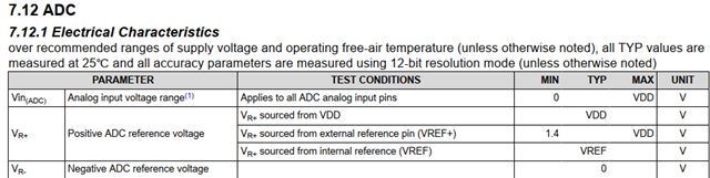
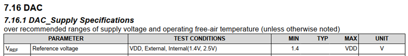
According to the datasheet, the analog input voltage should not exceed VDD. Also the reference voltage of the DAC supply should not exceed VDD.

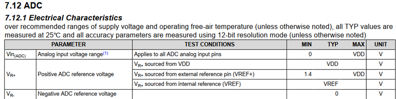
So, what happens to the ADC if the analog input voltage is greater than VDD?

Does the ADC measure incorrect values?

What happens to the DAC if the reference voltage is greater than VDD? Does it output a higher voltage than VDD?

Regards

  • Hi Sophie, in the case where you have your reference voltage set at a certain level from an external source, anything over that will essentially result in a value of 4096 with the 12 bit ADC. Since the voltage reference is correlated to the resolution (i.e 4096 would be 1.4V on the input with a 1.4V internal reference, or if the reference is 3.3V with the same 1.4V input, your ADC value would now be 1737). For the DAC, the output of the pin cannot be greater than the reference voltage. If you tried to increase, you would just see the voltage level stay at the maximum voltage based on VREF. Hope this helps!

    -Brian

  • Hi Brian,
    what happens if the positive ADC reference voltage (VR+) is greater than VDD?

  • The MSPM0's ADC is designed to operate within the limits set by VDD and ground (VSS). The datasheet will specify the absolute maximum ratings for voltage on any pin, including the VREF+ pin, which is typically VDD + 0.3V. Exceeding this limit is a violation of the device's operating conditions, so you could end up damaging the device by going over this limit.