Part Number: AM2634
Other Parts Discussed in Thread: AM263P4
Tool/software:
I have the same issues that were referenced but not resolved on another thread on this forum ( AM2632: ARM-Based MCU Can't Enter Boundary Scan Mode Using The AM263.bsdl ).
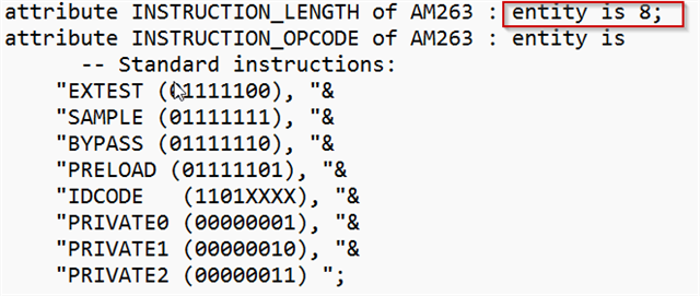
The supplied BSDL file for this device (AM2634CODFHAZCZR) specifies an 8 bit instruction register but when we capture the value of that register it only returns four bits.
We have also seen that the IDCode returned from the device has both a different version and part number value when compared to the value specified in the BSDL file.
As suggested in the previous thread we have tried different boot modes, and seen different behaviours. The behaviour described above was seen with bootmode 0110. When we tried with 1001, suggested in the other thread, we got no data returned from the chain. Neither of these boot modes is referenced in the TRM for the device.
Many thanks
Stuart