Part Number: TM4C1290NCPDT
Other Parts Discussed in Thread: EK-TM4C1294XL, TM4E129BNCZAD, , TM4C1294KCPDT
Tool/software:
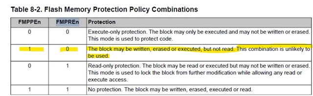
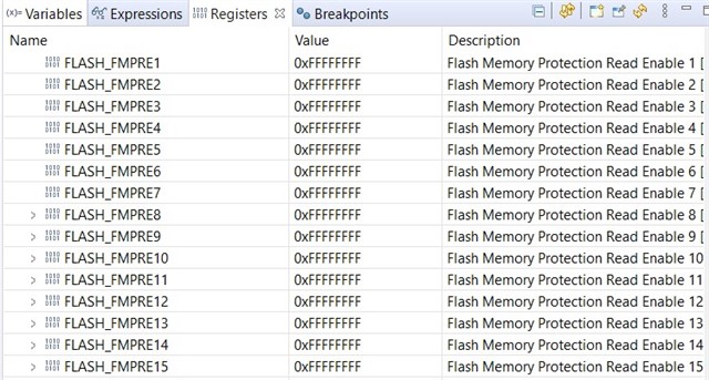
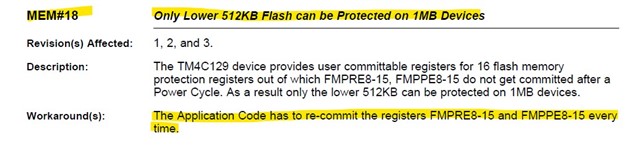
1、Chip registers FMPRE0 to FMPRE7 can be programmed, but data cannot be written to FMPRE8 to FMPRE15.
2、Chip registers FMPPE0 to FMPPE7 can be programmed, but data cannot be written to FMPPE8 to FMPPE15.
3、If the FMPRE0 register is fully set to 0, the chip will be permanently locked and cannot enter programming/debug mode again.