Part Number: AM263P4
Other Parts Discussed in Thread: SYSCONFIG
Tool/software:
Question 1:
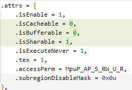
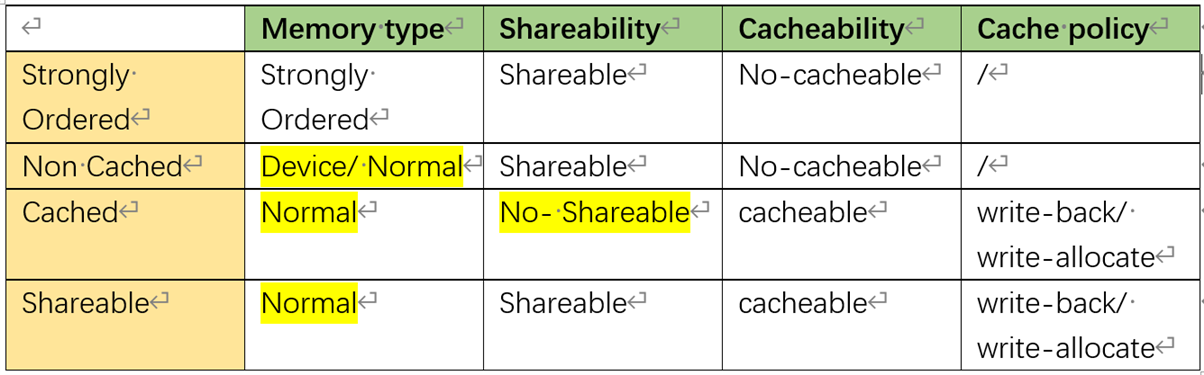
In the syscfg configuration of AM263P4, are the Region Attributes configurations limited to only certain combinations, rather than all possible combinations of Memory type, Shareability, Cacheability, and Cache policy?
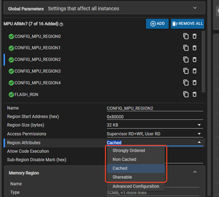
I would like to confirm whether my understanding of the Region Attributes combinations provided in syscfg is correct, particularly the highlighted entries.?
Question 2:
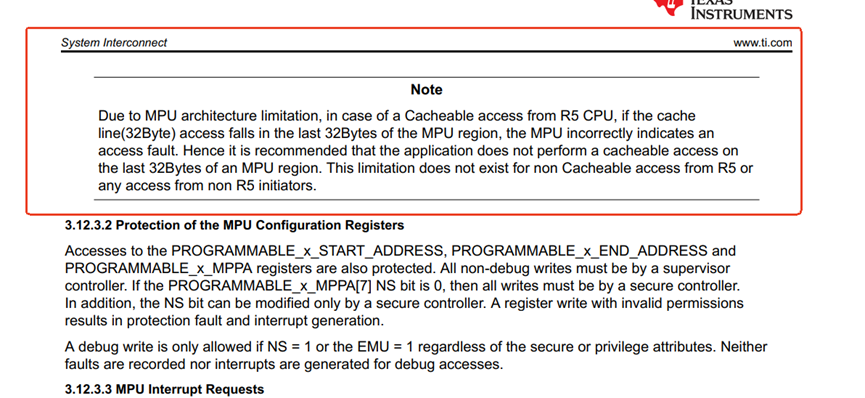
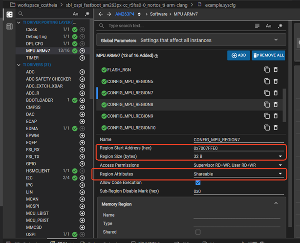
According to the TRM manual, the last 32 bytes of every 512KB must be configured as non-cached. However, in the fastboot example, this region is set to shareable. Isn't shareable equivalent to cached + shareable?
Question 3:
In the fastboot example, the RAM is configured as Cached. After performing relevant Flash operations, data consistency between the Cache and RAM is achieved using CacheP_wb to synchronize the data. In non-fastboot SBL (Secondary Boot Loader), the RAM region is configured as shareable. Given that shareable implies cached, does this also require the use of CacheP_wb to synchronize data between the Cache and RAM to ensure consistency?
If a region is configured as shareable, it allows multiple processing cores to share the data, whereas cached does not. Is this the reason why configuring the RAM region as cached prevents the R5 core from accessing OTP data? However, this raises another question: in the fastboot example, the RAM is set to Cached, so how can the HSM firmware read from Flash also be shared with the HSM core?
Question 4:
Does AM263P4 currently only support Write-Back and Write-Allocate cache policies? So, whenever the RAM region is configured as cached, data consistency can only be maintained through Write-Back. Does this mean that automatic data consistency can theoretically only be achieved via Write-Through? How can I determine which data will be processed by the Cache, i.e., when to perform manual data synchronization (Write-Back)?