AM2432: Profinet SYNC0_OUT signal remap

Part Number: AM2432

Tool/software:

Hello,

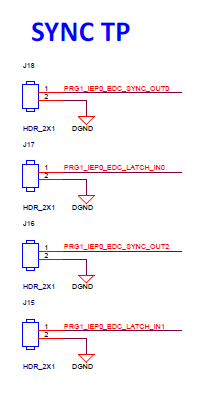
is it possible to remap the SYNC0_OUT signal to another pin?

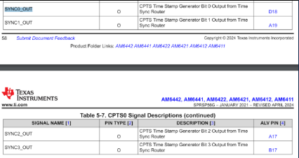
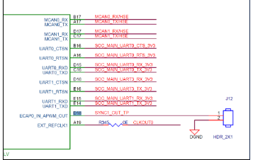
In the PN example (pn_app_iod_bsp.c), it is mapped to Ball.D18:

/*
 * PAD configuration for Ball.D18
 * Required to configure SYNC0_OUT as pin out
 */
static Pinmux_PerCfg_t gTsrPinMuxMainDomainCfg[] = {
    {
        PIN_ECAP0_IN_APWM_OUT,
        ( PIN_MODE(1) | PIN_PULL_DISABLE ) /* PIN_MODE 1 is SYNC0_OUT */
    },
    {PINMUX_END, PINMUX_END}
};

void PN_APP_IOD_tsrConfig(uint8_t syncSignal)
{
    Pinmux_config(gTsrPinMuxMainDomainCfg, PINMUX_DOMAIN_ID_MAIN);
    /* PRU IEP Enable SYNC MODE */
    CSL_REG32_WR(CSL_PRU_ICSSG1_PR1_CFG_SLV_BASE + CSL_ICSSCFG_IEPCLK, 1);
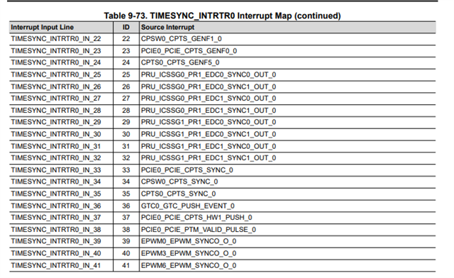
    CSL_REG32_WR(CSL_TIMESYNC_EVENT_INTROUTER0_CFG_BASE + 0x64, 0x0001001D + syncSignal);
}

Ideally to Ball.B16 (UART0_CTS_N)?

I tried to find information in the Technical Reference Manual, but I am confused.

Regards,
Vaclav

  • Hello Vaclav,

    It is currently not possible to map the sync signals (SYNC0 and SYNC1) to any pin on the board.

    1. You could use the pins that are present for both sync0 and sync1 signals on the board as mentioned in the schematics.

    2. Or it would be possible to route the sync signals to the following pins mentioned in the response to the below query.

     RE: AM2432: [Time Sync Router] SORTE_G/Device: How to select and enable the event? 

    Kindly reach out to us know if you require any further inputs on this topic.

    Best Regards,
    Laxman

  • Hello Laxman,
    Thank you for your reply.


    However, I cannot access the link in point 2:
    Access Denied
    You do not have permission to perform the requested action.


    Could you please make it accessible to me?

    Best regards,
    Valcav

  • Hi Vaclav,

    Sharing the steps mentioned to route sync signals.

    You can follow the steps mentioned below to enable the time sync router for SYNC0 signal.

    1. List of time sync events:


    2. List of output pins which the above mentioned time sync events can be mapped to:
    3. The above mentioned output pins are mapped to the following ball numbers
    4. Only Ball number D18 has been bought out and connected to the pin J12 on the AM243x-EVM. The rest of the ball numbers are not connected to any output pins.


      1. Hence, the SYNC0 signal can be routed to the J12 pin

    Regards,

    Laxman

  • Hello Laxman,

    we are trying to map synchronization signal to A19 which is only accessible ball on our HW which we can tie this function to. So we changed pin to PIN_EXT_REFCLK1 and used SYNC1, which didn't work. Now we are trying to understand registers for timesync event to find why we can't move same functionality from D18 to A19. 

    We tried to move register offset from 0x64 to another values (0x60, 0x68 and 0x6C as we found). Also we are trying to change the value of register according to this table.


    So we now have these functions 

    static Pinmux_PerCfg_t gTsrPinMuxMainDomainCfg[] = {
        {
        	PIN_EXT_REFCLK1,
            ( PIN_MODE(1) | PIN_PULL_DISABLE ) /* PIN_MODE 1 is SYNC0_OUT */
        },
        {PINMUX_END, PINMUX_END}
    };
    
    void PN_APP_IOD_tsrConfig(uint8_t syncSignal)
    {
        Pinmux_config(gTsrPinMuxMainDomainCfg, PINMUX_DOMAIN_ID_MAIN);
        /* PRU IEP Enable SYNC MODE */
        CSL_REG32_WR(CSL_PRU_ICSSG1_PR1_CFG_SLV_BASE + CSL_ICSSCFG_IEPCLK, 1);
        CSL_REG32_WR(CSL_TIMESYNC_EVENT_INTROUTER0_CFG_BASE + 0x6C, 0x0001001E);
    }

    Do you have idea, why we can't find any signal after making changes?

    Best regards,

    Jan

  • Hello Laxman,

    looks like we managet to solve this issue with this setting: 

    CSL_REG32_WR(CSL_TIMESYNC_EVENT_INTROUTER0_CFG_BASE + 0x68, 0x0001001D);

    Best regards,

    Jan