


Other Parts Discussed in Thread: SEGGER, TMDSCNCD263P, AM263P4
Tool/software:
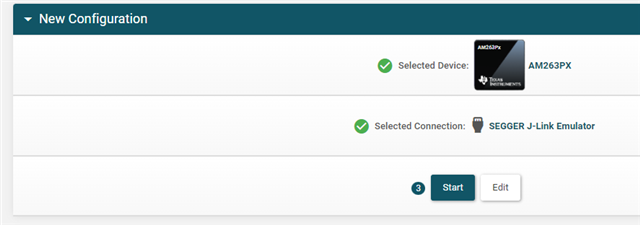
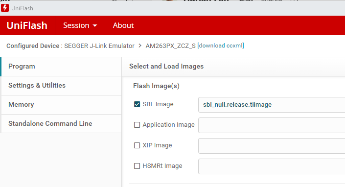
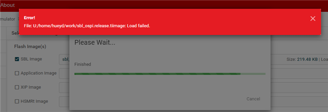
Trying to use Uniflash 9.3 with Segger J-Link Basic probe to program TMDSCNCD263P Rev A board but fails trying to program prebuild SBL image.
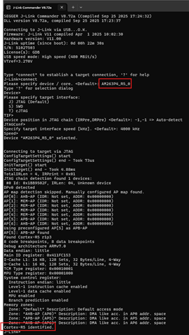
Installed SEGGER v8.72a. The connection seems to be correct (see J-LinkCommander log below).
When loading program, it complains "AM263PX" (or other variants) is unknown to this version of J-Link Software.
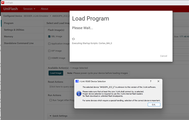
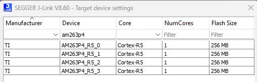
After selecting AM263P4_R5_0, the load proceeded then failed trying to program.
Log:
[9/29/2025, 2:25:07 PM] [INFO] Cortex_R5_0: GEL Output: Gel files loading Complete
[9/29/2025, 2:26:58 PM] [INFO] Cortex_R5_0: GEL Output: ***OnTargetConnect() Launched***
[9/29/2025, 2:26:58 PM] [INFO] Cortex_R5_0: GEL Output: AM263Px Initialization Scripts Launched. Please Wait...
[9/29/2025, 2:26:58 PM] [INFO] Cortex_R5_0: GEL Output: AM263Px_Cryst_Clock_Loss_Status() Launched
[9/29/2025, 2:26:58 PM] [INFO] Cortex_R5_0: GEL Output: Crystal Clock present
[9/29/2025, 2:26:58 PM] [INFO] Cortex_R5_0: GEL Output: AM263Px_SOP_Mode() Launched
[9/29/2025, 2:26:58 PM] [INFO] Cortex_R5_0: GEL Output: SOP MODE = 0x00000003
[9/29/2025, 2:26:58 PM] [INFO] Cortex_R5_0: GEL Output: OSPI (8S) - Octal Read Mode
[9/29/2025, 2:26:58 PM] [INFO] Cortex_R5_0: GEL Output: AM263Px_Read_Device_Type() Launched
[9/29/2025, 2:26:58 PM] [INFO] Cortex_R5_0: GEL Output: EFuse Device Type Value = 0x000000AA
[9/29/2025, 2:26:58 PM] [INFO] Cortex_R5_0: GEL Output: AM263Px_dual_or_lockstep_mode() Launched
[9/29/2025, 2:26:58 PM] [INFO] Cortex_R5_0: GEL Output: r5fss0 = 0x00000001
[9/29/2025, 2:26:58 PM] [INFO] Cortex_R5_0: GEL Output: r5fss1 = 0x00000000
[9/29/2025, 2:26:58 PM] [INFO] Cortex_R5_0: GEL Output: R5FSS0 is in Dual-Core mode
[9/29/2025, 2:26:58 PM] [INFO] Cortex_R5_0: GEL Output: R5FSS1 is in Dual-Core mode
[9/29/2025, 2:26:58 PM] [INFO] Cortex_R5_0: GEL Output: MSS_CTRL Control Registers Unlocked
[9/29/2025, 2:26:58 PM] [INFO] Cortex_R5_0: GEL Output: MSS_TOP_RCM Control Registers Unlocked
[9/29/2025, 2:26:58 PM] [INFO] Cortex_R5_0: GEL Output: MSS_RCM Control Registers Unlocked
[9/29/2025, 2:26:58 PM] [INFO] Cortex_R5_0: GEL Output: MSS_IOMUX Control Registers Unlocked
[9/29/2025, 2:26:58 PM] [INFO] Cortex_R5_0: GEL Output: TOP_CTRL Control Registers Unlocked
[9/29/2025, 2:26:58 PM] [INFO] Cortex_R5_0: GEL Output: *** R5FSS0 DualCore Reset ***
[9/29/2025, 2:26:58 PM] [INFO] Cortex_R5_0: GEL Output: *** R5FSS1 DualCore Reset ***
[9/29/2025, 2:26:58 PM] [INFO] Cortex_R5_0: GEL Output: R5F ROM Eclipse
[9/29/2025, 2:26:58 PM] [INFO] Cortex_R5_0: GEL Output: R5FSS0_0 Released
[9/29/2025, 2:26:58 PM] [INFO] Cortex_R5_0: GEL Output: R5FSS0_1 Released
[9/29/2025, 2:26:58 PM] [INFO] Cortex_R5_0: GEL Output: R5FSS1_0 Released
[9/29/2025, 2:26:58 PM] [INFO] Cortex_R5_0: GEL Output: R5FSS1_1 Released
[9/29/2025, 2:26:58 PM] [INFO] Cortex_R5_0: GEL Output: L2 Mem Init Complete
[9/29/2025, 2:26:58 PM] [INFO] Cortex_R5_0: GEL Output: MailBox Mem Init Complete
[9/29/2025, 2:26:58 PM] [INFO] Cortex_R5_0: GEL Output: r5fss0 = 0x00000001
[9/29/2025, 2:26:58 PM] [INFO] Cortex_R5_0: GEL Output: r5fss1 = 0x00000000
[9/29/2025, 2:26:58 PM] [INFO] Cortex_R5_0: GEL Output: R5FSS0 is in Dual-Core mode
[9/29/2025, 2:26:58 PM] [INFO] Cortex_R5_0: GEL Output: R5FSS1 is in Dual-Core mode
[9/29/2025, 2:26:58 PM] [INFO] Cortex_R5_0: GEL Output: CORE PLL Configuration Complete
[9/29/2025, 2:26:58 PM] [INFO] Cortex_R5_0: GEL Output: SYS_CLK DIVBY2
[9/29/2025, 2:26:58 PM] [INFO] Cortex_R5_0: GEL Output: DPLL_CORE_HSDIV0_CLKOUT0 selected as CLK source for R5FSS & SYS CLKs
[9/29/2025, 2:26:58 PM] [INFO] Cortex_R5_0: GEL Output: CLK Programmed R5F=400MHz and SYS_CLK=200MHz
[9/29/2025, 2:26:58 PM] [INFO] Cortex_R5_0: GEL Output: Configure all Peripheral clocks()
[9/29/2025, 2:26:58 PM] [INFO] Cortex_R5_0: GEL Output: *** Enabling Peripheral Clocks ***
[9/29/2025, 2:26:58 PM] [INFO] Cortex_R5_0: GEL Output: Enabling RTI[0:3] Clocks
[9/29/2025, 2:26:58 PM] [INFO] Cortex_R5_0: GEL Output: RTI0 Clock Enabled (200MHz)
[9/29/2025, 2:26:58 PM] [INFO] Cortex_R5_0: GEL Output: RTI1 Clock Enabled (200MHz)
[9/29/2025, 2:26:58 PM] [INFO] Cortex_R5_0: GEL Output: RTI2 Clock Enabled (200MHz)
[9/29/2025, 2:26:58 PM] [INFO] Cortex_R5_0: GEL Output: RTI3 Clock Enabled (200MHz)
[9/29/2025, 2:26:58 PM] [INFO] Cortex_R5_0: GEL Output: Enabling RTI_WDT[0:3] Clocks
[9/29/2025, 2:26:58 PM] [INFO] Cortex_R5_0: GEL Output: WDT0 Clock Enabled (200MHz)
[9/29/2025, 2:26:58 PM] [INFO] Cortex_R5_0: GEL Output: WDT1 Clock Enabled (200MHz)
[9/29/2025, 2:26:58 PM] [INFO] Cortex_R5_0: GEL Output: WDT2 Clock Enabled (200MHz)
[9/29/2025, 2:26:58 PM] [INFO] Cortex_R5_0: GEL Output: WDT3 Clock Enabled (200MHz)
[9/29/2025, 2:26:59 PM] [INFO] Cortex_R5_0: GEL Output: Enabling UART[0:5]/LIN[0:5] Clocks
[9/29/2025, 2:26:59 PM] [INFO] Cortex_R5_0: GEL Output: LIN0_UART0 Clock Enabled (160MHz)
[9/29/2025, 2:26:59 PM] [INFO] Cortex_R5_0: GEL Output: LIN1_UART1 Clock Enabled (160MHz)
[9/29/2025, 2:26:59 PM] [INFO] Cortex_R5_0: GEL Output: LIN2_UART2 Clock Enabled (160MHz)
[9/29/2025, 2:26:59 PM] [INFO] Cortex_R5_0: GEL Output: LIN3_UART3 Clock Enabled (160MHz)
[9/29/2025, 2:26:59 PM] [INFO] Cortex_R5_0: GEL Output: LIN4_UART4 Clock Enabled (160MHz)
[9/29/2025, 2:26:59 PM] [INFO] Cortex_R5_0: GEL Output: LIN5_UART5 Clock Enabled (160MHz)
[9/29/2025, 2:26:59 PM] [INFO] Cortex_R5_0: GEL Output: Enabling OSPI Clocks
[9/29/2025, 2:26:59 PM] [INFO] Cortex_R5_0: GEL Output: OSPI0 Clock Enabled (133MHz)
[9/29/2025, 2:26:59 PM] [INFO] Cortex_R5_0: GEL Output: Enabling I2C Clocks
[9/29/2025, 2:26:59 PM] [INFO] Cortex_R5_0: GEL Output: I2C Clock Enabled (48MHz)
[9/29/2025, 2:26:59 PM] [INFO] Cortex_R5_0: GEL Output: Enabling TRACE Clocks
[9/29/2025, 2:26:59 PM] [INFO] Cortex_R5_0: GEL Output: Trace Clock Enabled (250MHz)
[9/29/2025, 2:26:59 PM] [INFO] Cortex_R5_0: GEL Output: Enabling MCAN[0:3] Clocks
[9/29/2025, 2:26:59 PM] [INFO] Cortex_R5_0: GEL Output: MCAN0 Clock Enabled (80MHz)
[9/29/2025, 2:26:59 PM] [INFO] Cortex_R5_0: GEL Output: MCAN1 Clock Enabled (80MHz)
[9/29/2025, 2:26:59 PM] [INFO] Cortex_R5_0: GEL Output: MCAN2 Clock Enabled (80MHz)
[9/29/2025, 2:26:59 PM] [INFO] Cortex_R5_0: GEL Output: MCAN3 Clock Enabled (80MHz)
[9/29/2025, 2:26:59 PM] [INFO] Cortex_R5_0: GEL Output: Enabling MMCSD Clocks
[9/29/2025, 2:26:59 PM] [INFO] Cortex_R5_0: GEL Output: MMCSD Clock Enabled (48MHz)
[9/29/2025, 2:26:59 PM] [INFO] Cortex_R5_0: GEL Output: Enabling MCSPI[0:4] Clocks
[9/29/2025, 2:26:59 PM] [INFO] Cortex_R5_0: GEL Output: MCSPI0 Clock Enabled (48MHz)
[9/29/2025, 2:26:59 PM] [INFO] Cortex_R5_0: GEL Output: MCSPI1 Clock Enabled (48MHz)
[9/29/2025, 2:26:59 PM] [INFO] Cortex_R5_0: GEL Output: MCSPI2 Clock Enabled (48MHz)
[9/29/2025, 2:26:59 PM] [INFO] Cortex_R5_0: GEL Output: MCSPI3 Clock Enabled (48MHz)
[9/29/2025, 2:26:59 PM] [INFO] Cortex_R5_0: GEL Output: MCSPI4 Clock Enabled (48MHz)
[9/29/2025, 2:26:59 PM] [INFO] Cortex_R5_0: GEL Output: Enabling CONTROLSS Clocks
[9/29/2025, 2:26:59 PM] [INFO] Cortex_R5_0: GEL Output: CONTROLSS Clock Enabled (400MHz)
[9/29/2025, 2:26:59 PM] [INFO] Cortex_R5_0: GEL Output: Enabling CPTS Clocks
[9/29/2025, 2:26:59 PM] [INFO] Cortex_R5_0: GEL Output: CPTS Clock Enabled (250MHz)
[9/29/2025, 2:26:59 PM] [INFO] Cortex_R5_0: GEL Output: Enabling RGMI[5,50,250] Clocks
[9/29/2025, 2:26:59 PM] [INFO] Cortex_R5_0: GEL Output: RGMII5 Clock Enabled (5MHz)
[9/29/2025, 2:26:59 PM] [INFO] Cortex_R5_0: GEL Output: RGMII50 Clock Enabled (50MHz)
[9/29/2025, 2:26:59 PM] [INFO] Cortex_R5_0: GEL Output: RGMII250 Clock Enabled (250MHz)
[9/29/2025, 2:26:59 PM] [INFO] Cortex_R5_0: GEL Output: Enabling XTAL_TEMPSENSE_32K Clocks
[9/29/2025, 2:26:59 PM] [INFO] Cortex_R5_0: GEL Output: TEMPSENSE Clock Enabled (32KHz)
[9/29/2025, 2:26:59 PM] [INFO] Cortex_R5_0: GEL Output: Enabling XTAL_MMC_32K Clocks
[9/29/2025, 2:26:59 PM] [INFO] Cortex_R5_0: GEL Output: XTAL_MMC Clock Enabled (32KHz)
[9/29/2025, 2:26:59 PM] [INFO] Cortex_R5_0: GEL Output: ***All IP Clocks are Enabled***
[9/29/2025, 2:26:59 PM] [INFO] Cortex_R5_0: GEL Output: CPU reset (soft reset) has been issued through GEL on program load.
[9/29/2025, 2:27:02 PM] [ERROR] Cortex_R5_0: Trouble Writing Memory Block at 0x60027fb0 on Page 0 of Length 0x463c: Flash download failed! ...
[9/29/2025, 2:27:02 PM] [ERROR] Cortex_R5_0: File Loader: Verification failed: Target failed to write 0x60027FB0
Jlink is connected properly through TMDSHECDOCK and LED on probe is solid green. Using J-Link Commander, this shows probe is connected properly.
Can an expert help guide me through this process? I'm not sure where I went wrong here.
Thank you for the support.