This thread has been locked.

If you have a related question, please click the "Ask a related question" button in the top right corner. The newly created question will be automatically linked to this question.

TMDSCNCD263P: ECP: AM263P CC Inconsistency in Enabling 8D-8D-8D protocol in OSPI

Part Number: TMDSCNCD263P
Other Parts Discussed in Thread: SYSCONFIG

Hi Team,

Greetings of the day.

I’m currently working on the XIP feature using OSPI in 8D-8D-8D mode. To enable the required configuration, I followed the settings mentioned in the SDK’s SBL_OSPI_Multicore_elf example project and replicated the same steps in my custom bare-metal project.

While debugging the bare-metal code, I manually wrote some hardcoded values to the registers using the memory browser window. After issuing the Read Device ID command, I was able to successfully read both the Device ID and Manufacturer ID. Using a pointer to the flash address range, I was also able to read the correct data stored in the flash memory.

However, when I run the same code without step-by-step debugging (i.e., in one go), it does not work reliably. Sometimes it directly enters the while(1) loop, and at other times it gets stuck while reading the status register—the status register value remains 0xFF, and the code never exits from that state.

Could you please help me identify what might be causing this inconsistent behavior?

  • While debugging the bare-metal code, I manually wrote some hardcoded values to the registers using the memory browser window.

    What registers were modified here ?

    However, when I run the same code without step-by-step debugging (i.e., in one go), it does not work reliably. Sometimes it directly enters the while(1)

    What does the while(1) loop mean ?

    Also how are you debgging and running the procject ? Are you developing a boot loader application ?

    Will it be possible for you to share the code as it is a bit difficult to point out the issue in this context.

    Regards,

    Aswin

  • What registers were modified here ?

    After initializing the OSPI in MCU, then i reset the flash device and i called an API were NOR flash will get configured.

    overview of the code is 

    main()

    {

    //clock config to 133 Mhz

    //OSPI config

    config_nor_flash();

    while(1);

    }

    int32 config_not_flash()

    {

    uint32_t flash_data[8]={0};
    volatile uint32_t *flash_ptr = (unsigned int *)0x60000000U;

    //Transition from 1S to 8D mode

    0x8090=0x06000001; write en
    0x8090=0x05800001; read SR reg

    //read volatile reg,IO mode
    0x8094 = 0x0;
    0x8090 = 0x858A0401;//for 3 addr byte mode and 0x90= 0x858B0401; //for 4 byte addr mode;data available in 0xA0

    //mode transition to 8D if read reg value is not 0xE7

    0x8094 = 0;
    0x80A8 = E7;
    0x8090 = 0x810A8001;//here addr bytes =3,D.cy=0

    //immediately change OSPI to 8D, enable DTR in config reg, data lines to 8 in instr rd/wr reg and en ddr in rd reg
    0x8000 = 24th bit 1;
    0x8004 = 0x1003377c;
    0x8008 = 0x33084;
    0x8010 = 1 or 3

    //read back IO mode
    0x8094 = 0x0;
    0x8090 = 0x858A0401;//for 3 addr byte mode or 0x90= 0x858B0401; //for 4 byte addr mode;data available in 0xA0

    //now change dummy cycles to 16 in flash dev
    0x8090=0x06000001; write en
    0x8090=0x05800401; read SR reg

    0x8094 = 1;
    0x80A8 = 0x10;//16 dummy cycles
    0x8090 = 0x810A8001;//addr byte =3,D.cy=0

    //now change address bytes to 4 in flash dev
    0x8090=0x06000001; write en
    0x8090=0x05800401; read SR reg

    0x8094 = 0x5;
    0x80A8 = FE;
    0x8090 = 0x810A8001;//addr byte =3,D.cy=0
    and
    0x8014 = 0x3 {bits 3:0};

    ospi_set_transfer_opcodes(0x7c,0x84);

    ospi_set_dummy_cycles(16);

    flash_data[0] = flash_ptr[0];
    flash_data[1] = flash_ptr[0];
    flash_data[2] = flash_ptr[0];
    flash_data[3] = flash_ptr[0];
    flash_data[4] = *(unsigned int *)0x60080004U;
    flash_data[5] = *(unsigned int *)0x60081000U;

    }

    when i tried reading the flash data at 0x60000000 multiple times, the data data in variable flash_data[0 to 3] is different that mean the data at location kept read different for every read transaction.

    then i tried to read device id of the flash by issuing the cmd 0x9FB00401, but data received in different order

    Thanks in advance...

  • Hi Sanith,

    Since you have mentioned that it works while debugging step by step but not when running, then this commonly indicates to a delay problem.  In the SDK, you can see we are always reading the WIP status bit and then moving forward between commands.

    This logic would be required in your case. So it is required to have a delay between execution of commands.

    Regards,

    Aswin

  • Since you have mentioned that it works while debugging step by step but not when running, then this commonly indicates to a delay problem.  In the SDK, you can see we are always reading the WIP status bit and then moving forward between commands.

    As you mentioned to take care of WIP bit status, I ported entire SDK code to my custom project, then i'm initializing the OSPI peripheral in MCU and OSPI NOR Flash in 8D and 4Byte address mode.

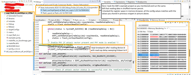
    I kept break point after reading device ID, but i got that device id in shuffled order at address 0x538080A0 location, what might be the reason?

  • Why the data received is not in proper order?

    In Read device id API they are checking for manufacture ID at index 0 and device id at index 1 and 2.

    so i got return value as SystemP_FAILURE

  • How does the shuffled order look ?

    What should be the man id and device id in your case. How is it looking compared to how it should ?

    Where you able to run the SDK example on your flash on custom board ?

    Can you see if the sysconfig configurations/register configurations are identical in the ported project as well (comparing with SDK example).

    Regards,

    Aswin

  • How does the shuffled order look ?

    in picture you can have a look, it looks like 0x195A9D10(4 bytes, even number of bytes is 8D mode)

    What should be the man id and device id in your case.

    man id is 0x9D and device id is 0x5A19

    Where you able to run the SDK example on your flash on custom board ?

    My custom board is not yet fabricated, so time being  i'm using AM263px CC eval board.

    SDK's SBL_OSPI_multicore elf example is working fine.

    in my custom project i ported SDK's example files and API's things are working as expected in 1S-1S-1S mode.{read dev id expected is 0x00195A9D 3 bytes}

    when i change mode to 8D, i observe this behavior and reading phy attackvector also getting failed

    Can you see if the sysconfig configurations/register configurations are identical in the ported project as well (comparing with SDK example).

    In my custom project i need to remove the dependency of sysconfig.

    All the code or logic should be bare metal with out any library or generated code

  • I kept break point after reading device ID, but i got that device id in shuffled order at address 0x538080A0 location, what might be the reason?

    Hi Sanith,

    Thank you for sharing the memory browser snippet.

    I noticed that the read data capture delay is currently set to 0. Could you please confirm whether you've tested the device ID read with different read data capture delay values? The shuffled byte order you're observing is typically caused by incorrect read data capture delay (tap) programming.

    Standard initialization sequence:

    1. Read data capture delay is typically initialized to a value of 8
    2. The code iteratively checks the device ID at different delay values
    3. The loop exits once the correct device ID is successfully read at a particular delay setting

    Recommendation: Could you try sweeping through different read data capture delay values (e.g., 0-15) and check at which value the device ID reads correctly? This will help identify the optimal tap setting for your hardware configuration.

    Please let me know the results, and we can proceed accordingly.

    Best regards,
    Mayank Shadwani

  • I noticed that the read data capture delay is currently set to 0. Could you please confirm whether you've tested the device ID read with different read data capture delay values? The shuffled byte order you're observing is typically caused by incorrect read data capture delay (tap) programming.

    Hi Mayank,

    You can see a while loop where the read capture delay is initialized to 8 and gradually decremented in each iteration. The loop terminates either when the delay value reaches zero or when the device ID is read successfully. The same logic is implemented here, as shown in the SDK example.

  • You can see a while loop where the read capture delay is initialized to 8 and gradually decremented in each iteration. The loop terminates either when the delay value reaches zero or when the device ID is read successfully. The same logic is implemented here, as shown in the SDK example.

    Hi Sanith,

    Thank you for the clarification regarding the while loop implementation.

    Could you please log the device ID value read at each read data capture delay setting? This will help us determine:

    1. Whether the correct device ID appears at any delay value within the current range (0-8)
    2. The pattern of device ID values across different delay settings

    If the correct device ID doesn't appear in the 0-8 range, please try expanding the search range by modifying the initialization from 8 to 15, allowing the loop to sweep through delay values 15 down to 0. This extended range may capture the optimal delay setting for your hardware configuration.

    Could you also confirm the following configuration parameters:

    • OSPI input clock frequency
    • Baud rate divider settings

    These parameters directly impact the optimal read data capture delay, and confirming them will help us narrow down the root cause.

    Looking forward to your findings.

    Best regards,
    Mayank

  • Could you please log the device ID value read at each read data capture delay setting? This will help us determine:

    1. Whether the correct device ID appears at any delay value within the current range (0-8)
    2. The pattern of device ID values across different delay settings

    If the correct device ID doesn't appear in the 0-8 range, please try expanding the search range by modifying the initialization from 8 to 15, allowing the loop to sweep through delay values 15 down to 0. This extended range may capture the optimal delay setting for your hardware configuration.

    Hi Mayank,

    As you said i logged the dev id read values for both 8 to 0 and 15 to 0

    the above is the log values for various read data capture delay from 8 to 0, here index number represents read data capture delay

    i.e., Dev_id_log[8] is 0x01101900 that means for read data cap delay is 8 and Id read is 0x01101900 and so on.

    Similarly for values 15 down to 0 log values are shown in below image

    Note:-

    OSPI input clock is 133Mhz  and baud divisor is by 8

  • Hi Sanith,

    Thank you for providing the detailed device ID logs for both delay ranges (8→0 and 15→0).

    I can see that none of the read data capture delay values (0-15) are returning the correct device ID. This suggests a potential issue with the 8D-8D-8D mode transition.

    I performed the same device ID read command in baremetal code after switching to 8D-8D-8D mode, and it worked successfully with a read data capture delay range of 0-4. I've attached a screenshot showing the correct device ID read with these delay settings.

    Configuration Used:

    • OSPI input clock: 133 MHz
    • Baud divisor: 8
    • Effective OSPI clock: 133 MHz / 8 = 16.625 MHz
    • Mode: 8D-8D-8D (Octal DTR)

    Please verify the 8D-8D-8D mode switch by performing the following test:

    • Send the Write Enable (WREN) command in 8D-8D-8D mode
    • Read back the flash status register in 8D-8D-8D mode
    • Check if the WEL (Write Enable Latch) bit is successfully set

    Please share your findings, and I'll help you resolve this issue.

    Best regards,

    Mayank Shadwani

  • After protocol switch to 8D mode,4 addr byte mode, and configuring dummy cycle, i kept break point and issued WREN cmd in 8D mode read back Status reg in 8D mode i can see that WEL bit is not latched to 1.(WEL is 0)

  •   API calls and logics are as per SDK example code but i cant see the expected result 

  • Hi Sanith,

    Thank you for testing the Write Enable (WREN) command in 8D-8D-8D mode.

    The fact that the WEL (Write Enable Latch) bit remains 0 after issuing the WREN command in 8D mode strongly suggests that the protocol switch to 8D-8D-8D mode itself may have failed.

    Could you please provide a memory browser dump of the OSPI configuration register space captured immediately after sending the "switch to 8D" command (before issuing WREN)? This will help us confirm whether the OSPI controller is properly configured for 8D-8D-8D mode operation.

    Please share the memory dump, and we'll analyze the configuration to identify the root cause.

    Best regards,
    Mayank

  •    Here i attached the memory dump of OSPI internal registers value after writing 0xE7 to I/O mode volatile config register

  • Hi Sanith,

    Can you provide a snippet of your sysconfig for OSPI section?

    Thanks,

    Mayank Shadwani

  • actually in my custom project im not using any SYSCONFIG. Our project should be independent of SYSCONFIG we need bare metal logic or our own custom logic to be implemented in our project. 

    I copied the code(logic) and driver config structure from SDK example code "SBL_OSPI_MULTI_CORE_ELF"

  •   actually in my custom project im not using any SYSCONFIG. Our project should be independent of SYSCONFIG we need bare metal logic or our own custom logic to be implemented in our project. 

    I copied the code(logic) and driver config structure from SDK example code "SBL_OSPI_MULTI_CORE_ELF"

  • Hi Sanith,

    Can you please confirm if you have sent a WR_EN command before switching to 8D mode? If yes, then did you send a status read command to check if WR_EN was asserted before sending move to 8D command?

    After protocol switch to 8D mode,4 addr byte mode, and configuring dummy cycle, i kept break point and issued WREN cmd in 8D mode read back Status reg in 8D mode i can see that WEL bit is not latched to 1.(WEL is 0)

    Also, there is some mismatch in the configuration space. This shouldn't happen if everything is same as SDK driver. I run the same thing from my end, and it gives me correct device ID. Attached a snippet of my config space.

    Can you please check for the differences in the configuration?

    Best Regards,

    Mayank Shadwani

  • Can you please confirm if you have sent a WR_EN command before switching to 8D mode? If yes, then did you send a status read command to check if WR_EN was asserted before sending move to 8D command?

       Yes, this is working fine. I sent WREN and then read back status reg and WEL latched to 1 then im sending 0xE7 but it is not switching properly.

    I want to ask one thing what is "Dual byte opcode" do i really need to enable that?

    i can see that difference in configuration register 0x53808000.

    in my project it is keeping the value  0x801838C1 -> {Dual byte opcode diabled, and DAC mode enable at the time of switching to 8D mode}

    but in your project it is 0xC1183841 { Dual byte opcode enabled, and DAC mode disabled why is there any specific reason}

  • I run the same thing from my end, and it gives me correct device ID. Attached a snippet of my config space.

      Can i know which SDK example code your running in debug mode and how your running that code what are the boot switch positions on CC EVAL board, can u guide me through the steps so that i can also do that on my EVAL board.

    Coz i tried to load OSPI_FLASH_XIP SDK example in Dev boot mode but unable to load that projects .out file 

  • Also, there is some mismatch in the configuration space. This shouldn't happen if everything is same as SDK driver.

    For your reference i can give the config structures and values i used for OSPI and flash devices

    OSPI_Attrs gOspiAttrs[CONFIG_OSPI_NUM_INSTANCES] =
    {
         {
    .baseAddr = 0x53808000U,
    .dataBaseAddr = 0x60000000U,
    .protocol = OSPI_PROTO_8D_8D_8D,
    .inputClkFreq = 133333333U,
    .intrNum = 54U,
    .intrEnable = FALSE,
    .intrPriority = 4U,
    .dmaEnable = FALSE,
    .phyEnable = TRUE,
    .dacEnable = TRUE,
    .chipSelect = OSPI_CS0,
    .frmFmt = OSPI_FF_POL0_PHA0,
    .decChipSelect = OSPI_DECODER_SELECT4,
    .baudRateDiv = 8,
    .dmaRestrictedRegions = gOspiDmaRestrictRegions,
         .phyConfiguration = {
        .phaseDelayElement = 1,
        .phyControlMode = OSPI_FLASH_CFG_PHY_MASTER_CONTROL_REG_PHY_MASTER_MODE,
       .dllLockMode = OSPI_PHY_DLL_HALF_CYCLE_LOCK,
               .tuningWindowParams = {
               .txDllLowWindowStart = 0,
               .txDllLowWindowEnd = 48,
               .txDllHighWindowStart = 20,
               .txDllHighWindowEnd = 96,
               .rxLowSearchStart = 0,
               .rxLowSearchEnd = 40,
               .rxHighSearchStart = 10,
               .rxHighSearchEnd = 127,
               .txLowSearchStart = 0,
               .txLowSearchEnd = 64,
               .txHighSearchStart = 20,
               .txHighSearchEnd = 127,
               .txDLLSearchOffset = 8,
               .rxTxDLLSearchStep = 4,
               .rdDelayMin = 1,
               .rdDelayMax = 3,
              } 
         }
       },
    };

    /* FLASH Attrs */
    Flash_Attrs OSPI_FLASH_DEV_ATTRs =
    {
        .flashName = "IS25LX256",
        .deviceId = 0x5A19,
        .manufacturerId = 0x9D,
        .flashSize = 33554432,//32MB
        .blockCount = 256, //128KB * 256 = 32MB
        .blockSize = 131072,//128KB for "L" device
        .pageCount = 512,
        .pageSize = 256,//1 to 256 bytes perpage
        .sectorCount = 8192,
        .sectorSize = 4096,
        .phyTuningOffset = 0x80000,
    };

    /* FLASH DevConfig */
    Flash_DevConfig FlashDevCfg_IS25LX256 =
    {
         .cmdExtType = OSPI_CMD_EXT_TYPE_REPEAT,
         .enable4BAddr = TRUE,
         .addrByteSupport = 1,
         .fourByteAddrEnSeq = 0,
         .cmdWren = 0x06,
         .cmdRdsr = 0x05,
         .srWip = (1 << 0),
         .srWel = (1 << 1),
         .xspiWipRdCmd = 0x05,
         .xspiWipReg = 0x00000000,
         .xspiWipBit = (1 << 0),
         .resetType = 0x30,
         

         .eraseCfg = {
         .blockSize = 131072,
         .sectorSize = 4096,
         .cmdBlockErase3B = 0xD8,
         .cmdBlockErase4B = 0xDC,
         .cmdSectorErase3B = 0x20,
         .cmdSectorErase4B = 0x21,
         .cmdChipErase = 0xC7,
         },


         .idCfg = {//device id read cmd
         .cmd = 0x9F, /* Constant */
         .numBytes = 3,
         .dummy4 = 0,
         .dummy8 = 8,
         .addrSize = 0
         },


         .protocolCfg = {
         .protocol = FLASH_CFG_PROTO_8D_8D_8D,
         .isDtr = TRUE,
         .cmdRd = 0x7c,
         .cmdWr = 0x84,
         .modeClksCmd = 0,
         .modeClksRd = 0,
         .dummyClksCmd = 16,
         .dummyClksRd = 16,
         .enableType = 0,
         .enableSeq = 0x00,
         

         .protoCfg = {
         .isAddrReg = TRUE,
         .cmdRegRd = 0x85,
         .cmdRegWr = 0x81,
         .cfgReg = 0,
         .shift = 0,
         .mask = 0xff,
         .cfgRegBitP = 231,//0xE7=231 means octal ddr
         },


         .strDtrCfg = {
         .isAddrReg = TRUE,
         .cmdRegRd = 0x85,
         .cmdRegWr = 0x81,
         .cfgReg = 0x00000000,
         .shift = 255,
         .mask = 0xFF,
         .cfgRegBitP = 0,
         },


         .dummyCfg = {
         .isAddrReg = TRUE,
         .cmdRegRd = 0x85,
         .cmdRegWr = 0x81,
         .cfgReg = 1,
         .shift = 0,
         .mask = 0xff,
         .cfgRegBitP = 16,
         },
    },


    .flashWriteTimeout = 120,
    .flashBusyTimeout = 72000000,
    };

        Can u confirm whether these config values are correct or not.

    Note:- I disabled DMA mode, sine i dont want to use DMA in my application, {already im using DMA with my conventional single line SPI so we dont want to ise DMA with OSPI}

  • Hi Sanith,

    in my project it is keeping the value  0x801838C1 -> {Dual byte opcode diabled, and DAC mode enable at the time of switching to 8D mode}

    but in your

    You would need to have this dual byte opcode bit field enabled for 8D-8D-8D mode, as some of the flashes does require extended opcode (inverted or repeated) to be sent along with the command in 8D mode. Enabling DTR field is taken care in OSPI_lld_setProtocol api. 

    Regards,

    Mayank Shadwani

  •     Can u confirm whether these config values are correct or not.

    Hi Sanith,

    The configurations appear correct for IS25LX256 in Octal DDR mode.

    Regards,

    Mayank Shadwani

  • You would need to have this dual byte opcode bit field enabled for 8D-8D-8D mode, as some of the flashes does require extended opcode (inverted or repeated) to be sent along with the command in 8D mode

    How I will know that i need to enable Extended Opcode for my flash. I haven't noticed about extended opcode in IS25LX256 flash datasheet{correct me if im wrong or if i missed about that section in datasheet} so i disabled that in my code.

    In the code i saw that in "OSPI_programInstance" API they are disabling

    can i know where they are enabling dual byte opcode in SBL_OSPI_multi_core example project?

  •   Can i know which SDK example code your running in debug mode and how your running that code what are the boot switch positions on CC EVAL board, can u guide me through the steps so that i can also do that on my EVAL board.

    Hi Sanith,

    I am using ospi_flash_io example, with a SOP value of 0xB (4'b1011), which is Dev Boot mode.

    Regards,

    Mayank Shadwani

  • Can i know which SDK example code your running in debug mode and how your running that code what are the boot switch positions on CC EVAL board, can u guide me through the steps so that i can also do that on my EVAL board.

    Coz i tried to load OSPI_FLASH_XIP SDK example in Dev boot mode but unable to load that projects .out file 

      can you say about this, i want to give a try from my side on SDK example code

  • How I will know that i need to enable Extended Opcode for my flash. I haven't noticed about extended opcode in IS25LX256 flash datasheet{correct me if im wrong or if i missed about that section in datasheet} so i disabled that in my code.

    In the code i saw that in "OSPI_programInstance" API they are disabling

    can i know where they are enabling dual byte opcode in SBL_OSPI_multi_core example project?

    Hi Sanith,

    You are correct - there's no explicit "extended opcode" requirement in the IS25LX256 datasheet.

    What Extended/Dual Byte Opcode Does:

    • In DDR mode, sends the same opcode twice (sampled on rising & falling clock edges)
    • Generic driver feature for compatibility with various flash vendors

    Where it's enabled:

    Flash_norOspiSetProtocol() 
      → Flash_set888mode() 
        → OSPI_setProtocol() 
          → OSPI_lld_setProtocol() 
            → OSPI_lld_setDualOpCodeMode()
                → CSL_REG32_FINS(&pReg->CONFIG_REG, OSPI_FLASH_CFG_CONFIG_REG_DUAL_BYTE_OPCODE_EN_FLD, TRUE);

    IS25LX256 will work with repeated opcode (no harm). If device ID reads correctly, configuration is fine

    Regards,

    Mayank Shadwani

  •   can you say about this, i want to give a try from my side on SDK example code

    Hi Sanith,

    I am using ospi_flash_io example, with a SOP value of 0xB (4'b1011), which is Dev Boot mode. Can you explain what error you encountered when you say "unable to load projects .out file?

    Regards,

    Mayank Shadwani

  • I am using ospi_flash_io example, with a SOP value of 0xB (4'b1011), which is Dev Boot mode. Can you explain what error you encountered when you say "unable to load projects .out file?

     Even i tried the same SDK example code in DEV Boot mode.

    Error message is

    "Cortex_R5_0: Trouble Writing Memory Block at 0x0 on Page 0 of Length 0x40: (Error -1065 @ 0x40) Unable to access device memory. Verify that the memory address is in valid memory. If error persists, confirm configuration, power-cycle board, and/or try more reliable JTAG settings (e.g. lower TCLK). (Emulation package 12.7.0.00105)
    Cortex_R5_0: File Loader: Verification failed: Target failed to write 0x00000000
    Cortex_R5_0: GEL: File: C:\workspace_v12\ospi_flash_io_am263px-cc_r5fss0-0_nortos_ti-arm-clang\Debug\ospi_flash_io_am263px-cc_r5fss0-0_nortos_ti-arm-clang.out: Load failed."

  • Hi Sanith,

    Can you share the complete console logs? Does your GEL script prints the selected boot mode?

    Thanks,

    Mayank Shadwani

  •  

    Here is the complete Logs

    Cortex_R5_0: GEL Output: Gel files loading on R5F0 Complete
    Cortex_R5_0: GEL Output: ***OnTargetConnect() Launched***

    Cortex_R5_0: GEL Output: AM263Px Initialization Scripts Launched.
    Please Wait...


    Cortex_R5_0: GEL Output: AM263Px_Cryst_Clock_Loss_Status() Launched
    Cortex_R5_0: GEL Output: Crystal Clock present
    Cortex_R5_0: GEL Output: AM263Px_SOP_Mode() Launched
    Cortex_R5_0: GEL Output: SOP MODE = 0x00000003
    Cortex_R5_0: GEL Output:
    OSPI - 8S Functional boot mode
    Cortex_R5_0: GEL Output: AM263Px_Read_Device_Type() Launched
    Cortex_R5_0: GEL Output: EFuse Device Type Value = 0x000000AA
    Cortex_R5_0: GEL Output: AM263Px_dual_or_lockstep_mode() Launched
    Cortex_R5_0: GEL Output: r5fss0 = 0x00000001
    Cortex_R5_0: GEL Output: r5fss1 = 0x00000000
    Cortex_R5_0: GEL Output:
    R5FSS0 is in Dual core mode
    Cortex_R5_0: GEL Output:
    R5FSS1 is in Dual core mode
    Cortex_R5_0: GEL Output: MSS_CTRL Control Registers Unlocked
    Cortex_R5_0: GEL Output: MSS_TOP_RCM Control Registers Unlocked
    Cortex_R5_0: GEL Output: MSS_RCM Control Registers Unlocked
    Cortex_R5_0: GEL Output: MSS_IOMUX Control Registers Unlocked
    Cortex_R5_0: GEL Output: TOP_CTRL Control Registers Unlocked
    Cortex_R5_0: GEL Output:

    *** R5FSS0 Reset DualCore ***
    Cortex_R5_0: GEL Output:

    ***R5FSS1 Reset DualCore ***
    Cortex_R5_0: GEL Output: R5F ROM Eclipse
    Cortex_R5_0: GEL Output: R5FSS0_0 Released
    Cortex_R5_0: GEL Output: R5FSS0_1 Released
    Cortex_R5_0: GEL Output: R5FSS1_0 Released
    Cortex_R5_0: GEL Output: R5FSS1_1 Released
    Cortex_R5_0: GEL Output: L2 Mem Init Complete
    Cortex_R5_0: GEL Output: MailBox Mem Init Complete
    Cortex_R5_0: GEL Output: *********** R5FSS0/1 Dual Core mode Configured********
    Cortex_R5_0: GEL Output: SYS_CLK DIVBY2
    Cortex_R5_0: GEL Output: DPLL_CORE_HSDIV0_CLKOUT0 selected as CLK source for R5FSS & SYS CLKs
    Cortex_R5_0: GEL Output:
    CLK Programmed R5F=400MHz and SYS_CLK=200MHz
    Cortex_R5_0: GEL Output:

    *** Enabling Peripheral Clocks ***
    Cortex_R5_0: GEL Output: Enabling RTI[0:3] Clocks
    Cortex_R5_0: GEL Output: Enabling RTI_WDT[0:3] Clocks
    Cortex_R5_0: GEL Output: Enabling UART[0:5]/LIN[0:5] Clocks
    Cortex_R5_0: GEL Output: Enabling QSPI Clocks
    Cortex_R5_0: GEL Output: Enabling I2C Clocks
    Cortex_R5_0: GEL Output: Enabling TRACE Clocks
    Cortex_R5_0: GEL Output: Enabling MCAN[0:3] Clocks
    Cortex_R5_0: GEL Output: Enabling MMCSD Clocks
    Cortex_R5_0: GEL Output: Enabling MCSPI[0:4] Clocks
    Cortex_R5_0: GEL Output: Enabling CONTROLSS Clocks
    Cortex_R5_0: GEL Output: Enabling CPTS Clocks
    Cortex_R5_0: GEL Output: Enabling RGMI[5,50,250] Clocks
    Cortex_R5_0: GEL Output: Enabling XTAL_TEMPSENSE_32K Clocks
    Cortex_R5_0: GEL Output: Enabling XTAL_MMC_32K Clocks
    Cortex_R5_0: GEL Output:

    ***All IP Clocks are Enabled***

    Cortex_R5_0: AM263Px
    Cortex_R5_0: Trouble Writing Memory Block at 0x0 on Page 0 of Length 0x40: (Error -1065 @ 0x40) Unable to access device memory. Verify that the memory address is in valid memory. If error persists, confirm configuration, power-cycle board, and/or try more reliable JTAG settings (e.g. lower TCLK). (Emulation package 12.7.0.00105)
    Cortex_R5_0: File Loader: Verification failed: Target failed to write 0x00000000
    Cortex_R5_0: GEL: File: C:\workspace_v12\ospi_flash_io_am263px-cc_r5fss0-0_nortos_ti-arm-clang\Debug\ospi_flash_io_am263px-cc_r5fss0-0_nortos_ti-arm-clang.out: Load failed."

  • Cortex_R5_0: GEL Output: AM263Px_SOP_Mode() Launched
    Cortex_R5_0: GEL Output: SOP MODE = 0x00000003
    Cortex_R5_0: GEL Output:
    OSPI - 8S Functional boot mode

    Hi Sanith,

    Looks like SOP mode is not correctly latched from the pins. Please check if SOP switches are physically set to 1011 (Dev Boot mode).

    Thanks,

    Mayank Shadwani

  • Looks like SOP mode is not correctly latched from the pins. Please check if SOP switches are physically set to 1011 (Dev Boot mode).

    But i physically changed the boot switches to Dev mode...

    after changing the pins i pressed power Reset button in the board...

    Do i need to do any hard power cycle?

  • Yes, please disconnect power source, wait for capacitors to discharge (typically 5-10 seconds) and then reconnect power.

  •  

    Hi mayank,

    Yeah did as suggested now i can able to load the code. I have gone through the code flow in debug mode step by step and tried to read the device ID,

    but ended up reading the data is same shuffled manner. Here attached the screen shot for your reference.

    Note:- I didn't modify any of the code/line in the SDK example project, just imported, compiled and ran the code that's it

    Thanks in advance...

  • Hi Sanith,

    Could you please provide the following information:

    1. Board Revision: Which board are you using - REV E1 or REV E2?

      • You can find this marking near the TEXAS INSTRUMENTS logo on the board.
    2. SDK Version: Which SDK version are you currently working with?

    This information will help us better assist you with your issue.

    Thanks,

    Mayank Shadwani

  • Hi ,

    On CC Board near Texas Instruments logo i checked and found something like this "PCB# PROC159B"

    and SDK version is "mcu_plus_sdk_am263px_11_00_00_19"

  • Cortex_R5_0: GEL Output: Enabling QSPI Clocks

    Hi Sanith,

    Could you please share your .ccxml file?

    It appears that incorrect GEL scripts may be configured in your target configuration, which could be causing clock configuration issues.

    Thanks,

    Mayank Shadwani

  •   Here i attached the screenshots of .ccxml file configurations

  • Hi Sanith,

    Can you please help us with the below details:

    1. Which version of CCS are you currently using? please use CCS12.8.1
    2. Also, can you please do "check for updates"  in Help and check any pending Sitara MCU Updates are present
      1. Restart CCS once updates are done.
      2. Create a new AM263Px ccxml. 

    Below is the expected gel output:

    Cortex_R5_0: GEL Output: Gel files loading Complete
    Cortex_R5_0: GEL Output: ***OnTargetConnect() Launched***
    
    Cortex_R5_0: GEL Output: AM263Px Initialization Scripts Launched. 
    Please Wait...
    
    
    Cortex_R5_0: GEL Output: AM263Px_Cryst_Clock_Loss_Status() Launched
    Cortex_R5_0: GEL Output: Crystal Clock present 
    Cortex_R5_0: GEL Output: AM263Px_SOP_Mode() Launched
    Cortex_R5_0: GEL Output: SOP MODE = 0x0000000B    
    Cortex_R5_0: GEL Output: Dev Boot Mode 
    Cortex_R5_0: GEL Output: AM263Px_Read_Device_Type() Launched
    Cortex_R5_0: GEL Output: EFuse Device Type Value = 0x000000AA    
    Cortex_R5_0: GEL Output: AM263Px_dual_or_lockstep_mode() Launched
    Cortex_R5_0: GEL Output: r5fss0 = 0x00000101    
    Cortex_R5_0: GEL Output: r5fss1 = 0x00000100    
    Cortex_R5_0: GEL Output: R5FSS0 is in Lockstep mode 
    Cortex_R5_0: GEL Output: R5FSS1 is in Lockstep mode 
    Cortex_R5_0: GEL Output: MSS_CTRL Control Registers Unlocked
    Cortex_R5_0: GEL Output: MSS_TOP_RCM Control Registers Unlocked
    Cortex_R5_0: GEL Output: MSS_RCM Control Registers Unlocked
    Cortex_R5_0: GEL Output: MSS_IOMUX Control Registers Unlocked
    Cortex_R5_0: GEL Output: TOP_CTRL Control Registers Unlocked
    Cortex_R5_0: GEL Output: *** R5FSS0 DualCore Reset ***
    Cortex_R5_0: GEL Output: *** R5FSS1 DualCore Reset ***
    Cortex_R5_0: GEL Output: R5F ROM Eclipse
    Cortex_R5_0: GEL Output: R5FSS0_0 Released
    Cortex_R5_0: GEL Output: R5FSS0_1 Released
    Cortex_R5_0: GEL Output: R5FSS1_0 Released
    Cortex_R5_0: GEL Output: R5FSS1_1 Released
    Cortex_R5_0: GEL Output: L2 Mem Init Complete
    Cortex_R5_0: GEL Output: MailBox Mem Init Complete
    Cortex_R5_0: GEL Output: r5fss0 = 0x00000001    
    Cortex_R5_0: GEL Output: r5fss1 = 0x00000000    
    Cortex_R5_0: GEL Output: R5FSS0 is in Dual-Core mode 
    Cortex_R5_0: GEL Output: R5FSS1 is in Dual-Core mode 
    Cortex_R5_0: GEL Output: CORE PLL Configuration Complete
    Cortex_R5_0: GEL Output: PER PLL Configuration Complete
    Cortex_R5_0: GEL Output: SYS_CLK DIVBY2
    Cortex_R5_0: GEL Output: DPLL_CORE_HSDIV0_CLKOUT0 selected as CLK source for R5FSS & SYS CLKs
    Cortex_R5_0: GEL Output: CLK Programmed R5F=400MHz and SYS_CLK=200MHz 
    Cortex_R5_0: GEL Output: Configure all Peripheral clocks()
    Cortex_R5_0: GEL Output: 
    
     *** Enabling Peripheral Clocks *** 
    Cortex_R5_0: GEL Output: Enabling RTI[0:3] Clocks 
    Cortex_R5_0: GEL Output: RTI0 Clock Enabled (200MHz)
    Cortex_R5_0: GEL Output: RTI1 Clock Enabled (200MHz)
    Cortex_R5_0: GEL Output: RTI2 Clock Enabled (200MHz)
    Cortex_R5_0: GEL Output: RTI3 Clock Enabled (200MHz)
    Cortex_R5_0: GEL Output: Enabling RTI_WDT[0:3] Clocks 
    Cortex_R5_0: GEL Output: WDT0 Clock Enabled (200MHz)
    Cortex_R5_0: GEL Output: WDT1 Clock Enabled (200MHz)
    Cortex_R5_0: GEL Output: WDT2 Clock Enabled (200MHz)
    Cortex_R5_0: GEL Output: WDT3 Clock Enabled (200MHz)
    Cortex_R5_0: GEL Output: Enabling UART[0:5]/LIN[0:5] Clocks 
    Cortex_R5_0: GEL Output: LIN0_UART0 Clock Enabled (160MHz)
    Cortex_R5_0: GEL Output: LIN1_UART1 Clock Enabled (160MHz)
    Cortex_R5_0: GEL Output: LIN2_UART2 Clock Enabled (160MHz)
    Cortex_R5_0: GEL Output: LIN3_UART3 Clock Enabled (160MHz)
    Cortex_R5_0: GEL Output: LIN4_UART4 Clock Enabled (160MHz)
    Cortex_R5_0: GEL Output: LIN5_UART5 Clock Enabled (160MHz)
    Cortex_R5_0: GEL Output: Enabling OSPI Clocks 
    Cortex_R5_0: GEL Output: OSPI0 Clock Enabled (133MHz)
    Cortex_R5_0: GEL Output: Enabling I2C Clocks 
    Cortex_R5_0: GEL Output: I2C Clock Enabled (48MHz)
    Cortex_R5_0: GEL Output: Enabling TRACE Clocks 
    Cortex_R5_0: GEL Output: Trace Clock Enabled (250MHz)
    Cortex_R5_0: GEL Output: Enabling MCAN[0:3] Clocks 
    Cortex_R5_0: GEL Output: MCAN0 Clock Enabled (80MHz)
    Cortex_R5_0: GEL Output: MCAN1 Clock Enabled (80MHz)
    Cortex_R5_0: GEL Output: MCAN2 Clock Enabled (80MHz)
    Cortex_R5_0: GEL Output: MCAN3 Clock Enabled (80MHz)
    Cortex_R5_0: GEL Output: Enabling MMCSD Clocks 
    Cortex_R5_0: GEL Output: MMCSD Clock Enabled (48MHz)
    Cortex_R5_0: GEL Output: Enabling MCSPI[0:4] Clocks 
    Cortex_R5_0: GEL Output: MCSPI0 Clock Enabled (48MHz)
    Cortex_R5_0: GEL Output: MCSPI1 Clock Enabled (48MHz)
    Cortex_R5_0: GEL Output: MCSPI2 Clock Enabled (48MHz)
    Cortex_R5_0: GEL Output: MCSPI3 Clock Enabled (48MHz)
    Cortex_R5_0: GEL Output: MCSPI4 Clock Enabled (48MHz)
    Cortex_R5_0: GEL Output: Enabling CONTROLSS Clocks 
    Cortex_R5_0: GEL Output: CONTROLSS Clock Enabled (400MHz)
    Cortex_R5_0: GEL Output: Enabling CPTS Clocks 
    Cortex_R5_0: GEL Output: CPTS Clock Enabled (250MHz)
    Cortex_R5_0: GEL Output: Enabling RGMI[5,50,250] Clocks 
    Cortex_R5_0: GEL Output: RGMII5 Clock Enabled (5MHz)
    Cortex_R5_0: GEL Output: RGMII50 Clock Enabled (50MHz)
    Cortex_R5_0: GEL Output: RGMII250 Clock Enabled (250MHz)
    Cortex_R5_0: GEL Output: Enabling XTAL_TEMPSENSE_32K Clocks 
    Cortex_R5_0: GEL Output: TEMPSENSE Clock Enabled (32KHz)
    Cortex_R5_0: GEL Output: Enabling XTAL_MMC_32K Clocks 
    Cortex_R5_0: GEL Output: XTAL_MMC Clock Enabled (32KHz)
    Cortex_R5_0: GEL Output: 
    
     ***All IP Clocks are Enabled*** 
    
    Cortex_R5_0: AM263Px
    Cortex_R5_0: Board Selected : CC
    Cortex_R5_0: Part Selected : Standard

    Regards,
    Rijohn

  • Which version of CCS are you currently using? please use CCS12.8.1

    Hi

    Thanks for letting me know about the recommended version.

    I’m currently using CCS version 12.7.0.

    Do I need to use exactly version 12.8.1, or will any version higher than 12.8.1 work?

  • Hi Sanith,

    Higher versions are also fine.You can use latest 20.x version.

    Regards,
    Rijohn

  •   

    Hi Team, 

    Which version of CCS are you currently using? please use CCS12.8.1

    I Installed CCS 12.8.1 version and created new target configuration ccxml file.

    Then i tried to debug but there is no change in console logs.

    I checked the version of sitara device support and Sitara MCU support software's installed, those are

    The logs are

    Cortex_R5_0: GEL Output: Gel files loading on R5F0 Complete
    Cortex_R5_0: GEL Output: ***OnTargetConnect() Launched***
    
    Cortex_R5_0: GEL Output: AM263Px Initialization Scripts Launched. 
    Please Wait...
    
    
    Cortex_R5_0: GEL Output: AM263Px_Cryst_Clock_Loss_Status() Launched
    Cortex_R5_0: GEL Output: Crystal Clock present 
    Cortex_R5_0: GEL Output: AM263Px_SOP_Mode() Launched
    Cortex_R5_0: GEL Output: SOP MODE = 0x0000000B    
    Cortex_R5_0: GEL Output: 
     Dev Boot Mode 
    Cortex_R5_0: GEL Output: AM263Px_Read_Device_Type() Launched
    Cortex_R5_0: GEL Output: EFuse Device Type Value = 0x000000AA    
    Cortex_R5_0: GEL Output: AM263Px_dual_or_lockstep_mode() Launched
    Cortex_R5_0: GEL Output: r5fss0 = 0x00000101    
    Cortex_R5_0: GEL Output: r5fss1 = 0x00000100    
    Cortex_R5_0: GEL Output: 
     R5FSS0 is in Lockstep mode 
    Cortex_R5_0: GEL Output: 
     R5FSS1 is in Lockstep mode 
    Cortex_R5_0: GEL Output: MSS_CTRL Control Registers Unlocked
    Cortex_R5_0: GEL Output: MSS_TOP_RCM Control Registers Unlocked
    Cortex_R5_0: GEL Output: MSS_RCM Control Registers Unlocked
    Cortex_R5_0: GEL Output: MSS_IOMUX Control Registers Unlocked
    Cortex_R5_0: GEL Output: TOP_CTRL Control Registers Unlocked
    Cortex_R5_0: GEL Output: 
    
    *** R5FSS0 DualCore Reset ***
    Cortex_R5_0: GEL Output: 
    
    ***R5FSS1 DualCore Reset ***
    Cortex_R5_0: GEL Output: R5F ROM Eclipse
    Cortex_R5_0: GEL Output: R5FSS0_0 Released
    Cortex_R5_0: GEL Output: R5FSS0_1 Released
    Cortex_R5_0: GEL Output: R5FSS1_0 Released
    Cortex_R5_0: GEL Output: R5FSS1_1 Released
    Cortex_R5_0: GEL Output: L2 Mem Init Complete
    Cortex_R5_0: GEL Output: MailBox Mem Init Complete
    Cortex_R5_0: GEL Output: *********** R5FSS0/1 Dual Core mode Configured********
    Cortex_R5_0: GEL Output: CORE PLL Configuration Complete
    Cortex_R5_0: GEL Output: PER PLL Configuration Complete
    Cortex_R5_0: GEL Output: SYS_CLK DIVBY2
    Cortex_R5_0: GEL Output: DPLL_CORE_HSDIV0_CLKOUT0 selected as CLK source for R5FSS & SYS CLKs
    Cortex_R5_0: GEL Output: 
     CLK Programmed R5F=400MHz and SYS_CLK=200MHz 
    Cortex_R5_0: GEL Output: 
    
     *** Enabling Peripheral Clocks *** 
    Cortex_R5_0: GEL Output: Enabling RTI[0:3] Clocks 
    Cortex_R5_0: GEL Output: Enabling RTI_WDT[0:3] Clocks 
    Cortex_R5_0: GEL Output: Enabling UART[0:5]/LIN[0:5] Clocks 
    Cortex_R5_0: GEL Output: Enabling QSPI Clocks 
    Cortex_R5_0: GEL Output: Enabling I2C Clocks 
    Cortex_R5_0: GEL Output: Enabling TRACE Clocks 
    Cortex_R5_0: GEL Output: Enabling MCAN[0:3] Clocks 
    Cortex_R5_0: GEL Output: Enabling MMCSD Clocks 
    Cortex_R5_0: GEL Output: Enabling MCSPI[0:4] Clocks 
    Cortex_R5_0: GEL Output: Enabling CONTROLSS Clocks 
    Cortex_R5_0: GEL Output: Enabling CPTS Clocks 
    Cortex_R5_0: GEL Output: Enabling RGMI[5,50,250] Clocks 
    Cortex_R5_0: GEL Output: Enabling XTAL_TEMPSENSE_32K Clocks 
    Cortex_R5_0: GEL Output: Enabling XTAL_MMC_32K Clocks 
    Cortex_R5_0: GEL Output: 
    
     ***All IP Clocks are Enabled*** 
    
    Cortex_R5_0: AM263Px
    Cortex_R5_0: Board Selected : CC
    Cortex_R5_0: Part Selected : Standard
    

    Can u let me know what are the things i missed

    Thanks in advance...

  • Hi Sanith,

    I noticed that your Sitara MCU Device support is showing version 1.3.8, but it should be 1.4.0 or higher for CCS 12.8.1.

    Could you please perform a "Check for Updates" after installing CCS 12.8.1? You can do this by:

    1. Going to the "Help" menu
    2. Selecting "Check for Updates"
    3. Installing any available updates
    4. Restarting CCS once the updates are complete

    This should resolve the version discrepancy.

    Best regards,
    Mayank Shadwani

  • Hi  

    I checked for updates it is showing no updates found.

    Can you check the available websites, do i need to check any website from here, bcz some are disabled

  • Hi Sanith,

    I've reviewed your setup and noticed that your "Available Software Sites" is displaying fewer options than expected. I've attached a screenshot from my CCS window so you can compare.

    Could you please try re-installing CCS 12.8.1? This should ensure that all the necessary software repositories are properly configured during installation.

    Please let me know if the issue persists after reinstalling.

    Best regards,
    Mayank Shadwani