Other Parts Discussed in Thread: SYSCONFIG
Dear TI support community,
I ran into a problem to calibrate the DAC output amplifier offset on MSPM0G3507. Below is some background information.
Background
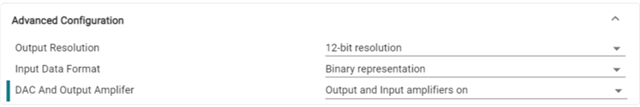
I tested the intergrated DAC on MSPM0G3507 lauchpad with the dac12_fixed_voltage_ref_internal example from the SDK. It outputs an offset at zero input, measuring about 7.2 mV on my lauchpad, which I would like to remove/reduce with user calibration per section 19.2.11 in the TRM. Using sysconfig, I setup the following: internal 1.4V voltage reference; CPUCLK = 4 MHz.
Detailed DAC sysconfig illustrated below:

Below is a code snippet for calibration - I am using MSPM0 SDK 2.7.0.05.
int main(void)
{
    uint32_t delay = 8000000;   // ~2 sec delay at 4 MHz CPUCLK frequency


    SYSCFG_DL_init();


    DL_DAC12_performSelfCalibrationBlocking(DAC0);

    DL_DAC12_setAmplifier(DAC0,DL_DAC12_AMP_ON); // Turn on output amplifier after calibration is completed
    DL_DAC12_enableOutputPin(DAC0);

    DL_DAC12_output12(DAC0, 0);     // initialise output to 0

...
}
Observations
The program run into an infinite loop at the DL_DAC12_performSelfCalibrationBlocking() line, due to DAC0_CTL0.CALON bit not automatically reset. Also, the CALDATA register is not being updated. In the meantime, the DAC output pin voltage fluctuates and then converges at ~2 mV.

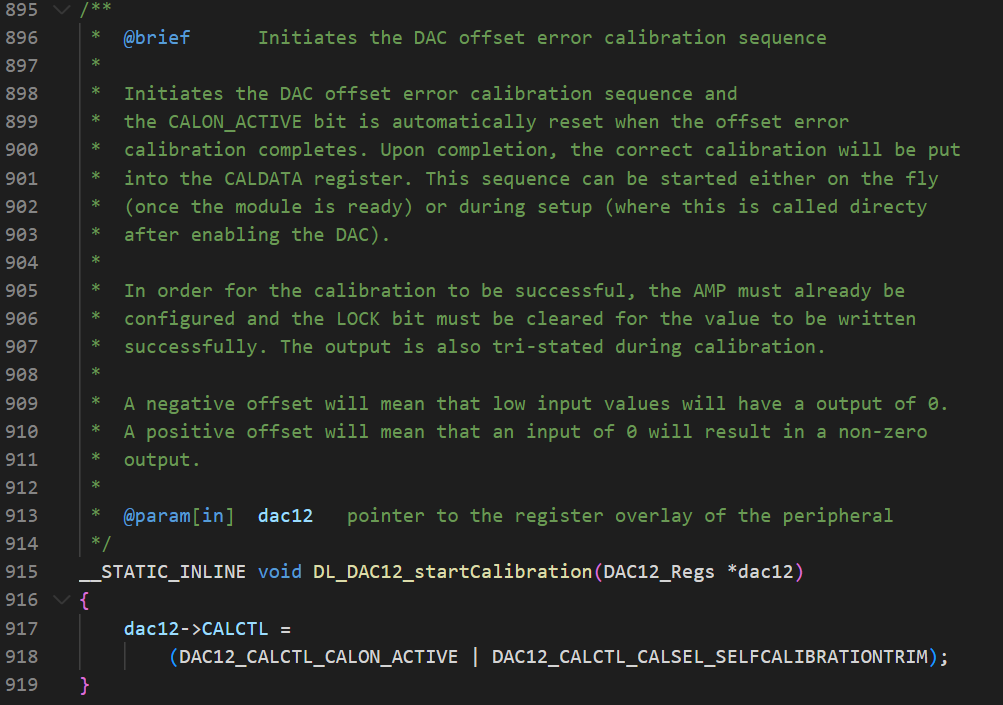
Further, referring to the DL_DAC12_startCalibration() function (referenced by DL_DAC12_performSelfCalibrationBlocking), in the description there is mentioning of the AMP and LOCK bits - I cannot find any reference to the latter in the DAC section of the TRM.
Questions
Is this a problem related to CPUCLK frequency selection and DAC reference configuration?
Could you please clarify how to correctly configure DAC output AMP settings to allow successful offset calibration? And, if relevant, how to configure the LOCK bit as described in the source code?
And finally, approximately how long does it normally take to perform calibration?
Kind regards,
Xuexi