Part Number: MSPM0G3507
Other Parts Discussed in Thread: SYSCONFIG
Hi,
I have two main questions right now regarding the SPI peripheral in the MSPM0G3507:
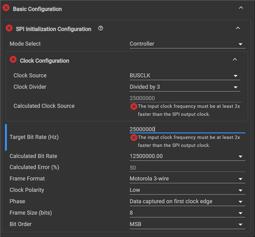
1 - Our SPI controller clock rate must be 25MHz and I'd like to run the MSPM0 at the highest CPU clock available given that contstraint. I have it running at 50MHz, which divides the SPI clock down to 25MHz and that's working as expected, but is there really no way to say set the BUSCLK to 75Mhz and divide it down to 25MHz? Or another way to increase MCLK from 50MHz and keep the SPI clock at 25MHz?
2 - I'd like to transfer fragmented blocks of memory out the SPI peripheral without CPU intervention. Does the MSPM0 DMA support linked list transfers to the SPI Tx register? Table mode seems perfect except that it's only capable of doing single transfers not block transfers. If there was a transfer size component, table mode would be perfect. Can I set the DMA into gather mode with different strides? Can I use a second DMA channel to 'feed' the primary DMA channel transfer configurations?
For example, I have a linked list of four data buffers:
Buffer 1 contains 10 bytes of SPI data (starting address 0x2000_1000)
Buffer 2 contains 4 bytes of SPI data (starting address 0x2000_1200)
Buffer 3 contains 512 bytes of SPI data (starting address 0x2000_1240)
Buffer 4 contains 4 bytes of SPI data (starting address 0x2000_2000)
Is the only way to acheive this functionality to do it in the SPI ISR? I have this working, but we're incuring 8uS to setup each transfer (MCLK is set to 50MHz) even with using the DriverLib APIs so in the above example the best case scenario will incur 32uS of transfer setup time.