TMDS273EVM: LVDS CBUFF example data rate & clock

Part Number: TMDS273EVM


Hello TI masters,

Im using the TMDS273EVM and my goal is to evaluate the LVDS interface by sending some buffers and monitor the signals with an oscilloscope.

Using the default example, i see that 2 lanes are selected and the configuration is 450 Mbps (225 MHz DDR Clock) by measuring the LVDS CLK_P and aligning it with the supported values from the TRM (SPRUIU0E):
LDVS_SUPPORTED_MODES.png

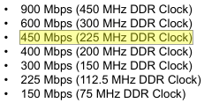
The example driver configures the HSI clock:

    /* Configure HSI interface Clock */
    HW_WR_REG32(CSL_MSS_TOPRCM_U_BASE + CSL_MSS_TOPRCM_HSI_CLK_SRC_SEL, 0x222);
    HW_WR_REG32(CSL_MSS_TOPRCM_U_BASE + CSL_MSS_TOPRCM_HSI_DIV_VAL, 0x333);


Here i need your help to interpret this right in order to use the other supported modes and data rates:

By navigating through the TRM and the clock architecture, i see that this utilizes the the Clock Source: PLL_DSP_CLK (0x222 -> 2):
image.png

The clock divider is 0x333->3:
image.png


  1. I cannot see a divider value 3 in this table, am i missing something?
  2. How the 225Mhz clock is generated with these settings (Source: 2, Divider:3)?
  3. I want to send multiple buffers sequentially, but when i activate/deactivate session in a loop, the code does not run as expected (only when i re-run the example again), so what is the best practice with this driver to treat continuous data streams?

Thanks in advance,
Konstantinos

  • Hi,

    The assigned expert is currently out of office, expect a delayed response. Please ping this thread if you do not hear back in 2-3 days.

    Regards,
    Johnson

  • Hi Konstantinos,

    1. The "0x333" for CSL_MSS_TOPRCM_HSI_DIV_VAL is the actual divider-1, so the actual divider here is 4: 1800/4 = 450Mhz

    2. To get 225Mhz, you will need to set the divider to 0x777 (8-1 = 7)

    3. For continuous processing, you will need two CBUFF_createSession(): one for Ping-buffer and one for Pong-buffer. You will need to activate/deactivate ping and pong buffers alternatively, so that the EDMA is filing one buffer, the DSP is processing the other.

    Best regards,

    Ming 

  • Sorry for my late reply,

    The default values of the example are HSI_SRC_SEL = 0x222 and HSI_DIV_VAL = 0x333.
    I measure the J7 PIN44 LVDS_CLK_P -> 225Mhz.
    Maybe there is another way to change the clock? Not only from these two lines? Can you please check the example provided?

    When i try other values for the HSI_SRC_SEL & HSI_DIV_VAL, i always measure 225Mhz.

  • Hi Konstantinos,

    As I mentioned in the previous post, if you set the HSI_DIV_VAL to 0x333, the HSI_CLK will be 450Mhz.

    If you set the HSI_DIV_VAL to 0x777, the HSI_CLK will be 225Mhz.

    According to the TRM table 11-1107, it seems the LVDS_CLK is set in CFG_LVDS_GEN_0:

    - Bit 14: CFG_LVDS_CLK_SEL and

    - Bit 21-16: CFG_LVDS_CLK_DIV

    Can you please check the value of CFG_LVDS_GEN_0 after the CBUFF settings?

    Best regards,

    Ming

  • With the default example the CFG_LVDS_GEN_0:
    (only difference is that i use one lane)

    CFG_LVDS_CLK_SEL :1
    CFG_LVDS_CLK_DIV: 2
    (same as yours)


        /* Configure HSI interface Clock */
        HW_WR_REG32(CSL_MSS_TOPRCM_U_BASE + CSL_MSS_TOPRCM_HSI_CLK_SRC_SEL, 0x222);
        HW_WR_REG32(CSL_MSS_TOPRCM_U_BASE + CSL_MSS_TOPRCM_HSI_DIV_VAL, 0x333);


    However i I measure the J7 PIN44 LVDS_CLK_P -> 225Mhz with the default settings above

    Additionally, if i change the values above CFG_LVDS_CLK_DIV, CSL_MSS_TOPRCM_HSI_CLK_SRC_SEL, CSL_MSS_TOPRCM_HSI_DIV_VAL, the measured clock does not change.
    The latest TRM is RevE and the CFG_LVDS_GEN_0 is on page 3126 - Table 11-864.

    So, how the HSI_CLK is related to the J7 PIN44 LVDS_CLK_P and what is the proper programming sequence to actually change it?


  • Hi Konstantinos,

    I cannot find the direct description about the relationship between the LVDS_CLK and the HSI_CLK in TRM, but the from the clues in the MCU+ SDK and TRM. The LVDS_CLK is either the HSI_CLK (SDR mode) or 1/2 of the HSI_CLK (DDR mode).

    Based on the value of CFG_LVDS_GEN_0 Bit 15 (cclksel1, 0-> Use div-by-2 [Q2 path]) and the Bit 10 (CFG_BIT_CLK_MODE, 1: DDR clocking mode). You are using the DDR mode, so the LVDS_CLK (225Mhz) is 1/2 of the HSI_CLK (450Mhz).

    You can try to change LVDS_CLK by change the Bit 15 to 1. Hopefully, you will get LVDS_CLK to 450Mhz.

    The CFG_LVDS_CLK_DIV is not used because the Bit 14 is set to 1: CLK_HSI_DIG is used, you can also try to set the Bit 14 (cclksel) to 0, then the CFG_LVDS_CLK_DIV will be used.

    If your target bit rate is 450Mbps (225Mhz DDR Clock), then the current CBUFF example has the right settings.

    Best regards,

    Ming