TMS570LC4357: Please clarify turnaround for EMIF access to 16bit NVRAM

Part Number: TMS570LC4357


Team,
Can you please help with the below questions.

Thanks in advance,
Anthony

TMS570LC4357 is connected to NVRAM, With EMIF as asynchronous memory with a 16-bit word width.

About Turnaround period:
-Under what conditions the turnaround is inserted?
Only when switching between read and write / write and read, or also between two read / two write accesses? 
Is there a difference between a 32-bit memory access (which then results in two 16-bit EMIF accesses) and two 16-bit memory accesses placed directly one after the other? 

-Where is the turnaround period is inserted?
On TRM SPNU563 page 814 it reads as if it is inserted before an EMIF access. 
However, Figure 21-32 on page 845 shows it after an access. 

-It is also unclear which register values lead to which setup, strobe, hold and turnaround times.
On TRM SPNU563 page 812, the term ‘minus one cycle’ is used in each case, so I would assume that a register value of 0, for example, leads to a setup time of one EMIF cycle. 
However, the information and diagrams on pages 812 and 845 partly contradict this theory. 
The turnaround period is particularly unclear to me in this context.

-We have also carried out tests with the EMIF interface, which have led to further questions. 
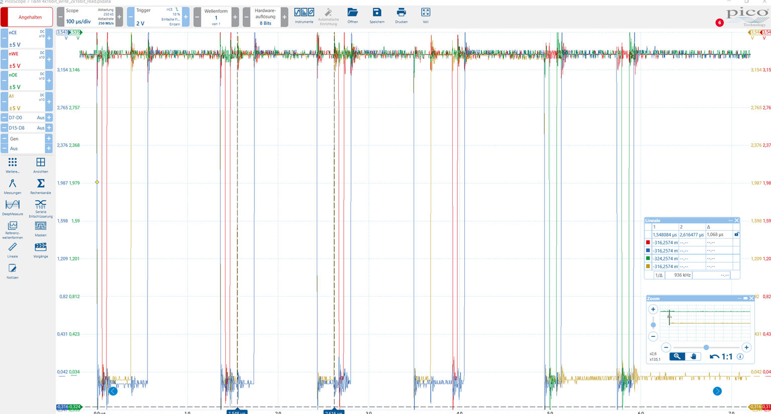
The interface was operated at 37.5 MHz and the associated configuration register (CE2CFG) was set to the value 0x04142111U. 
The following recording shows four 16-bit write accesses followed by two 16-bit read accesses:
 Wave1.png
The following code was executed for this:
code1.png

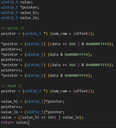
The two read accesses look as expected, but the four write accesses do not. 
It is noticeable that the chip select is pulled much earlier or remains pulled much longer than necessary. 
The address bit A1 also does not always behave as described in the TRM. 
Furthermore, the extremely long time between individual accesses is noticeable, varying between 613 ns and 1.068 µS (see rulers). 

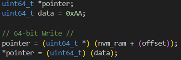
Another test was carried out, this time with a 64-bit write access:
Wave2.png

code2.png
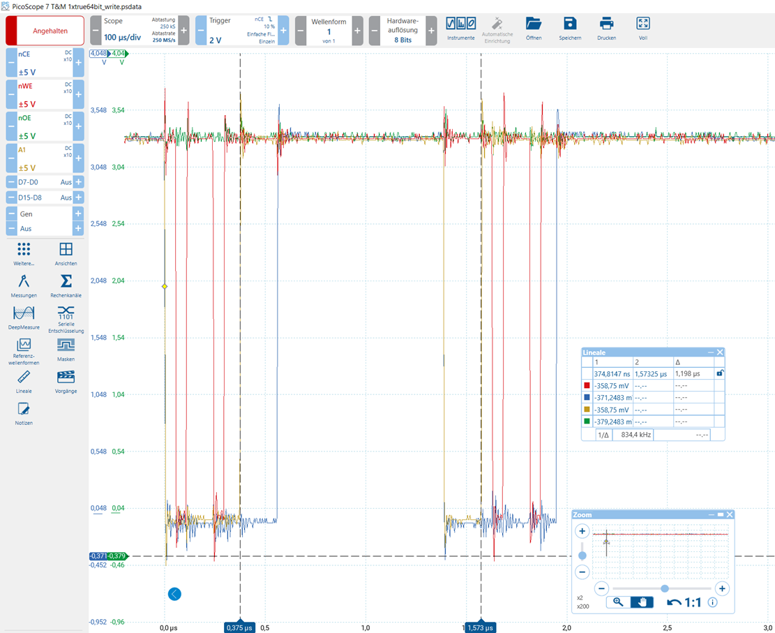
As expected for a 32-bit architecture, this access was divided into two 32-bit accesses. 

Each 32-bit access appears to consist of two 16-bit accesses directly strung together. 
However, this test again shows a very long time (1.198 µS) between the two 32-bit accesses. 

The questions that arise:
-How can the behaviour of the chip select during write accesses be explained, and can this be reconciled with the information from the TRM? 
-Is there a way to shorten the long wait time between individual 16/32-bit accesses in order to achieve a higher effective data rate?

  • HI,

    I will take a look

  • -Under what conditions the turnaround is inserted?

    The TA (turn-around) is the programable delay in clock cycles. The TA is to allow the external memory to prepare for the next operation. It's a mandatory pause between different types of memory transactions on the same chip select. 


    -Where is the turnaround period is inserted?

    It is inserted before the memory access

    If TA[3:2]=0, 1 cycle delay is inserted. or if you want to insert 3 cycles of delay, you need to program 3-1 (minus one cycles) to TA[3:2] filed. Some for other parameters (setup, hold, and strobe)

  • -How can the behaviour of the chip select during write accesses be explained, and can this be reconciled with the information from the TRM? 
    -Is there a way to shorten the long wait time between individual 16/32-bit accesses in order to achieve a higher effective data rate?

    For 16-bit data write, there is only one WE pulse in on CS period since only 1 bus transaction. For 32-bit data write, there are two WE pulses in one CS period because of of two bus transaction. 

    EMIF asynchronous interface can operate in either normal mode or select strobe mode. In normal mode the nCS will be active for the entire EMIF transaction. In select strobe mode the nCS is only active during the strobe time.

    In normal mode, the nCS is active for an entire EMIF bus transaction. For example, if you are writing to a EMIF address, the nCS is active for the entire bus transaction (16-bit write) while the nWE has two or three pulses while the nCS is active. This is the bug in revA silicon. However, in select strobe mode, the nCS is only active during the strobe phase which means that the nCS is actually active in phase with the nWE. While we see extra nWE pulses in normal mode we would also see extra nCS in select strobe mode.

    This bug has been fixed in revB and later rev silicon. The extra nWE pulses has been removed during write transactions. However, there was some technical difficulty to shorten the extra duration of the active nCS in addition to removing the extra WE pulses. When switched to select strobe mode, these extra duration of nCS remains as two extra nCS pulses. But the nWE and nOE are not active when these extra nCS pulses are active. So from a memory access stand point this should be fine. All writes and reads to the memory should be qualified with the valid nWE and nOE.

    For read, not only were we able to remove the extra nOE pulses but also to shorten the nCS as well to improve EMIF performance/bandwidth. Therefore, during read, there is no extra nOE or nCS pulses seen in either normal or select strobe mode.

    This extra CS duration will lower the throughput, but will not cause the data lost.

  • Hi,

    thank you for the replies (the question was originaly raised by me).

    I have two follow-up questions:

    1. Regarding the extra duration of nCS: In the worst case, how many EMIF clock cycles can the nCS be active for a 16-bit write access?

    2. Can you explain why there is such a long delay between two individual accesses? In the program code, only the pointer is incremented by one in the meantime. This should not lead to a delay of up to 1.2 µs, right?

    Thanks and regards,

    Johannes

  • Hi Johannes,

    The length of one CS can be calculated using the parameters (setup, strobe, hold) written in CE2CFG: (2+2+3)*EMIF clock cycles

    Three CS cycles is around 600ns.