This thread has been locked.

If you have a related question, please click the "Ask a related question" button in the top right corner. The newly created question will be automatically linked to this question.

AM2612: LP-AM261 Debug Issues When Trying to Enable XIP from OSPI Flash

Part Number: AM2612
Other Parts Discussed in Thread: LP-AM261, SYSCONFIG, UNIFLASH,

Hello E2E Experts,

I am trying the LP-AM261, trying to evaluate the performance in different scenarios of code and data placement.

I am using SysConfig 1.25.0 and SDK for AM261x 11.0.0.29.

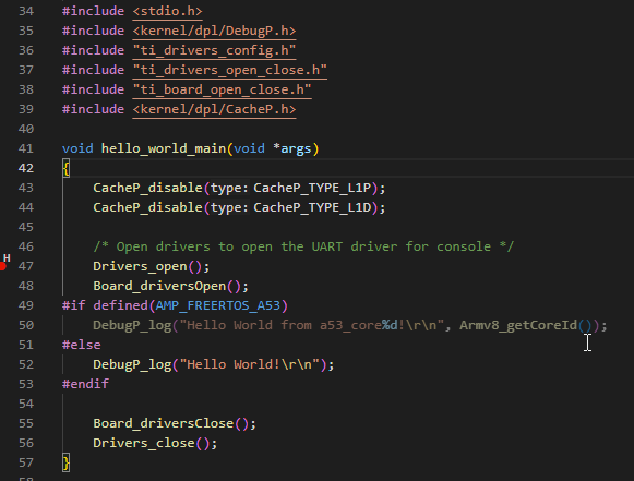
I started with the example \examples\drivers\gpio\gpio_led_blink\am261x-lp, where I was able to build, load and execute the example (code executed from OCRAM) successfully. At that time, I didn't know much of the boot process, so I don't exactly know exactly what were the BOOT pins nor the SBL loaded in the chip. Though I can guarantee the BOOT pins were not in UART mode, nor in xSPI mode.

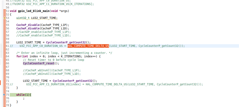
Then I stripped the code associated to LED blinking and added my code used for processors performance evaluation. I was able to build, load and execute successfully directly from CCS, with code executed from OCRAM. 

The next goal for me is to execute this code from external OSPI flash. I followed the steps explained  in https://dev.ti.com/tirex/explore/content/mcu_plus_sdk_am261x_10_00_01_10/docs/api_guide_am261x/BOOTFLOW_XIP.html and I was able to build the SW.

Trying to load the application from CCS did not work, but I'm pretty sure at some point I've seen logs in the Debug Output window with successfull flash programming, but on the page mentionned above, it is said you need a tool to flash the OSPI flash, so I used the uart_uniflash.py tool from \tools\boot in the SDK, using this .cfg file:

# First point to sbl_uart_uniflash binary, which function's as a server to flash one or more files
--flash-writer=sbl_prebuilt/am261x-lp/sbl_uart_uniflash.release.tiimage

# Program the OSPI PHY tuning attack vector
--operation=flash-phy-tuning-data

# When sending bootloader make sure to flash at offset 0x0. ROM expects bootloader at offset 0x0
--file=sbl_prebuilt/am261x-lp/sbl_ospi_multicore_elf.release.tiimage --operation=flash --flash-offset=0x0

# When sending application image, make sure to flash at offset 0x81000 (default) or to whatever offset your bootloader is configured for
--file=../../../../../workspace_ccstheia/gpio_led_blink_am261x-lp_r5fss0-0_nortos_ti-arm-clang/Release/gpio_led_blink_am261x-lp_r5fss0-0_nortos_ti-arm-clang.mcelf --operation=flash-sector-write --flash-offset=0x81000

# send the XIP image for this application, no need to specify flash offset since flash offset is specified within the image itself
--file=../../../../../workspace_ccstheia/gpio_led_blink_am261x-lp_r5fss0-0_nortos_ti-arm-clang/Release/gpio_led_blink_am261x-lp_r5fss0-0_nortos_ti-arm-clang.mcelf_xip --operation=flash-mcelf-xip

The flash programming succeeds and when I set BOOT pins to xSPI mode, I have the console displaying that all is OK:

xSPI_BOOT_SBL_Log.jpg

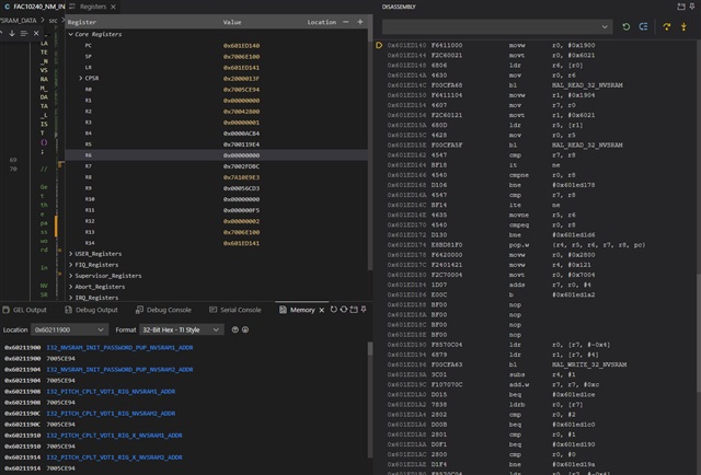
According to the page above, I figured to add the "loadSymbolsOnly" option in the launch.json file in order for the debugger not to try to flash when debug starts (in that case I was not able to only connect to the target). Once connected, I could get some performance measurement variables updated so I guess the code of my application was running OK. I was also able to change cache settings to evaluate performance with or without instruction and/or data cache.

Now, here are the issues I need help with (when running from flash and BOOT pins set to xSPI mode):

  • I don't understand why no breakpoint works.
  • I don't understand what the debugger does when I click the restart button, but apparently, it does nothing.
  • When I want to change cache settings (disable it, changing regions atributes to non-cacheable, forcing normal as write-through, etc...) through .syscfg file, or by defining my own ti_dpl_config.c file, I always find the core stuck in an abort or prefetch or undefined instruction exception. When I changed the parameter when running from OCRAM, I had no issue with this.
  • Is there a combination of BOOT mode pins and SBL that could make CCS able to program the flash and debug an application without the need of an other tool?

Any help would be appreciated. Thanks

  • Hi, just in case, here are some updates:

    • I found in the CCS options a way to disallow software breakpoints, as they were responsible of changing bits of programmed flash and caused undefined instruction exceptions.
    • I found the option, when connected to the probe, to only reset the core. After flashing, resetting the board in xSPI boot (with sbl_ospi_multicore_elf.release.tiimage) and after connecting to the probe, I still need to reboot the board so the SBL loads the R5 vectors in TCMA, else it is stuck to zero.
    • I noticed something else: when booting in xSPI mode, when I am in a debug session, the board appears to reset by itself from time to time. Do you have any idea why would this happen? Does the BOOT ROM setup a watchdog or anything like that?

    So now, my biggest problem is that when I put the code in flash, except the parts mentionned in the Enabling XIP or eXecute In Place, and if I disable L1D and L1P caches at the beginning of my first function executing from flash, I have a prefetch abort that I can not understand. I have checked the MPU configuration and it seems correct. The abort provides a fault adddress (IFAR) of 0x0317F10C, which doesn't match with anything from the Cortex-R5 manual, nor the ARM architecture reference manual, nor with my application linker .map file. The abort occurs when executing an instruction ldr pc pc,0 executed from flash.

    Does this mean something to you?

    Thanks, 

    • I don't understand why no breakpoint works.

    In XIP there is support only fot hardware breakpoints. Software break points are not supported.

    • I don't understand what the debugger does when I click the restart button, but apparently, it does nothing.

    To retsart the code, you would need to powercycle the board. In XIP, CCS is not used to load the code. It used as a tool just for debugging.

    When I want to change cache settings (disable it, changing regions atributes to non-cacheable, forcing normal as write-through, etc...) through .syscfg file, or by defining my own ti_dpl_config.c file, I always find the core stuck in an abort or prefetch or undefined instruction exception. When I changed the parameter when running from OCRAM, I had no issue with this.

    This behaviour is not actually expected. May I know if the below linker changes have been made ?

    Also to start with XIP could you please try with the examples\hello_world_xip_fss1  example in the SDK and see if you are able to debug this. I will upload a debug guide for CCS 20.4.0.

    Is there a combination of BOOT mode pins and SBL that could make CCS able to program the flash and debug an application without the need of an other tool?

    We cannot use any inbuilt options in CCS to program flash. The options are to use

    - UniFlash GUI

    - UART Uniflasher

    - CCS JTAG Uniflash Project.

    Please see the below documentation to know more.

    Regards,

    Aswin

  • Hi Gael,

    Please see the following the FAQ to setup XIP debug.

     [FAQ] AM2612-Q1: How to debug XIP application using CCS Theia 

    Do let me know if you have any questions.

    Regards,

    Aswin

  • Hi Aswin,

    Thank for the guide and your answers, but I am correct on all the points (linker, cache settings, removing anything that could install breakpoints, disallowing software breakpoints, ...).

    I added the infinite loop at the beginning of the loaded application and I can take control at this point with the debugger.

    I removed the GEL scripts to let the SBL boot, with BOOT pins in xSPI mode (but I understand I could use DevBoot mode with GEL scripts instead).

    At the beginning of my application, I disable the caches: 

        CacheP_disable(CacheP_TYPE_L1P);
        CacheP_disable(CacheP_TYPE_L1D);

    The issues I still have:

    • I observe certain errors occurring at specific addresses of the flash: once it was when branching to a specific location in the application (in flash) but getting a prefetch error with a weird instruction opcode. Now I modified the code, I get data abort error on a data that is not present at this location. In the screenshots: step 0: Before execution of code at 0x601ED140 and 0x601ED144 (move 0x60211900 in r0). Step1: r0 is loaded with 0x60211900 (see r6 equals 0; see data at address 0x60211900 is 0x7005CE94). Step2: when instruction ldr r6, [r0] is executed, r6 becomes 0x0004F2C7 instead of 0x7005CE94). I tried this without the memory view nor the disassembly view (to remove any debugger access to flash) but it does the same, and at the exact same place each time. If I modify the code, I think the error would be seen elsewhere and may lead to different kind of error.
    • When booting in xSPI mode and during debug, the board/cpu resets on its own. Is it normal? Is there a watchdog or something similar?
    • I lowered JTAG frequency to 1MHz as written somewhere in a guide, but I still have sometimes messages related to "Can not access the DAP, ....". I can still debug, but I mention it.

    With what I observe, I think this may be related to a misconfiguration of the flash by the SBL. I am using the prebuilt SBL from SDK 11.00.00.29:

    --file=sbl_prebuilt/am261x-lp/sbl_ospi_multicore_elf.release.tiimage --operation=flash --flash-offset=0x0

    If I use DevBOOT mode, is there a GEL script to use which also configures the OSPI flash in max speed mode?

    Thanks

    Step0:


    Step1:

    Step2:

  • I removed the GEL scripts to let the SBL boot, with BOOT pins in xSPI mode (but I understand I could use DevBoot mode with GEL scripts instead).

    Hi Gael, 

    We cannot use XIP in Dev Boot Mode. If you use Gel scripts then the peripherals would get reset. In XIP, when you are at the main() function, we need to OSPI and Flash to be initialized and functional. If Gels are there then this would not happen. So XIP debugging should be done only in OSPI/xSPI boot mode.

    At the beginning of my application, I disable the caches

    Is this the SDK example or the modified example as mentioned in the initial query?

    • When booting in xSPI mode and during debug, the board/cpu resets on its own. Is it normal? Is there a watchdog or something similar?

    No this is not expected at all. 

    Can you share me the project that you are using? If that is not possisble shall I take the hello word xip example add do cache disablement ?

    I would like to try this on my side. I am planning to use AM261 LP with macronix flash.

    Also may I know if the observations are the same without cache disablement as well ?

    Regards,

    Aswin

  • Hi Aswin,

    Ok for DevBoot mode, I didn't try this so I will stick to xSPI mode. Thanks for the clarification.

    I am using the gpio led blink example that I modified according to the page about enabling XIP mode, and added company code to run benchmarks.

    In order to share the project, I will prepare the exact same one without our company code and I will verify I still have the same issues before sending it to you (after he holidays).

    In the meantime, I can provide the configuration aspects of the projects. You'll see that I also had OCRAM region added for RL2, but in the sysconfig file I then disabled it.

    main.c:

    gpio_led_blink.c:

    ti_dpl_config.c (generated by CCS)

    /*
     *  Copyright (C) 2022 Texas Instruments Incorporated
     *
     *  Redistribution and use in source and binary forms, with or without
     *  modification, are permitted provided that the following conditions
     *  are met:
     *
     *    Redistributions of source code must retain the above copyright
     *    notice, this list of conditions and the following disclaimer.
     *
     *    Redistributions in binary form must reproduce the above copyright
     *    notice, this list of conditions and the following disclaimer in the
     *    documentation and/or other materials provided with the
     *    distribution.
     *
     *    Neither the name of Texas Instruments Incorporated nor the names of
     *    its contributors may be used to endorse or promote products derived
     *    from this software without specific prior written permission.
     *
     *  THIS SOFTWARE IS PROVIDED BY THE COPYRIGHT HOLDERS AND CONTRIBUTORS
     *  "AS IS" AND ANY EXPRESS OR IMPLIED WARRANTIES, INCLUDING, BUT NOT
     *  LIMITED TO, THE IMPLIED WARRANTIES OF MERCHANTABILITY AND FITNESS FOR
     *  A PARTICULAR PURPOSE ARE DISCLAIMED. IN NO EVENT SHALL THE COPYRIGHT
     *  OWNER OR CONTRIBUTORS BE LIABLE FOR ANY DIRECT, INDIRECT, INCIDENTAL,
     *  SPECIAL, EXEMPLARY, OR CONSEQUENTIAL DAMAGES (INCLUDING, BUT NOT
     *  LIMITED TO, PROCUREMENT OF SUBSTITUTE GOODS OR SERVICES; LOSS OF USE,
     *  DATA, OR PROFITS; OR BUSINESS INTERRUPTION) HOWEVER CAUSED AND ON ANY
     *  THEORY OF LIABILITY, WHETHER IN CONTRACT, STRICT LIABILITY, OR TORT
     *  (INCLUDING NEGLIGENCE OR OTHERWISE) ARISING IN ANY WAY OUT OF THE USE
     *  OF THIS SOFTWARE, EVEN IF ADVISED OF THE POSSIBILITY OF SUCH DAMAGE.
     */
    /*
     * Auto generated file
     */
    #include <stdio.h>
    #include <drivers/soc.h>
    #include <kernel/dpl/AddrTranslateP.h>
    #include "ti_dpl_config.h"
    #include "ti_drivers_config.h"
    
    
    /* ----------- HwiP ----------- */
    HwiP_Config gHwiConfig = {
        .intcBaseAddr = 0x50F00000u,
    };
    
    /* ----------- ClockP ----------- */
    #define RTI0_CLOCK_SRC_MUX_ADDR (0x53208140u)
    #define RTI0_CLOCK_SRC_WUCPUCLK (0x0u)
    #define RTI0_BASE_ADDR     (0x52180000u)
    
    uint32_t gR5ClockFrequency = SOC_RCM_R5_FREQ_500MHZ;
    
    ClockP_Config gClockConfig = {
        .timerBaseAddr = RTI0_BASE_ADDR, 
        .timerHwiIntNum = 124,
        .timerInputClkHz = 25000000,
        .timerInputPreScaler = 1,
        .usecPerTick = 1000,
        .intrPriority = 15,
        .isPulseInterrupt = 1,
    };
    
    /* ----------- DebugP ----------- */
    void putchar_(char character)
    {
        /* Output to CCS console */
        putchar(character);
        /* Output to UART console */
        DebugP_uartLogWriterPutChar(character);
    }


    #define RODATA_CFG_SECTION __attribute__((section(".rodata.cfg")))
    /* ----------- CacheP ----------- */
    const CacheP_Config gCacheConfig RODATA_CFG_SECTION = {
        .enable = 1,
        .enableForceWrThru = 0,
    };
    
    /* ----------- MpuP_armv7 ----------- */
    #define CONFIG_MPU_NUM_REGIONS  (5u)
    
    const MpuP_Config gMpuConfig RODATA_CFG_SECTION = {
        .numRegions = CONFIG_MPU_NUM_REGIONS,
        .enableBackgroundRegion = 0,
        .enableMpu = 1,
    };
    
    const MpuP_RegionConfig gMpuRegionConfig[CONFIG_MPU_NUM_REGIONS] RODATA_CFG_SECTION =
    {
        {
            .baseAddr = 0x0u,
            .size = MpuP_RegionSize_2G,
            .attrs = {
                .isEnable = 1,
                .isCacheable = 0,
                .isBufferable = 0,
                .isSharable = 1,
                .isExecuteNever = 1,
                .tex = 0,
                .accessPerm = MpuP_AP_S_RW_U_R,
                .subregionDisableMask = 0x0u
            },
        },
        {
            .baseAddr = 0x0u,
            .size = MpuP_RegionSize_32K,
            .attrs = {
                .isEnable = 1,
                .isCacheable = 1,
                .isBufferable = 1,
                .isSharable = 0,
                .isExecuteNever = 0,
                .tex = 1,
                .accessPerm = MpuP_AP_S_RW_U_R,
                .subregionDisableMask = 0x0u
            },
        },
        {
            .baseAddr = 0x80000u,
            .size = MpuP_RegionSize_32K,
            .attrs = {
                .isEnable = 1,
                .isCacheable = 1,
                .isBufferable = 1,
                .isSharable = 0,
                .isExecuteNever = 0,
                .tex = 1,
                .accessPerm = MpuP_AP_S_RW_U_R,
                .subregionDisableMask = 0x0u
            },
        },
        {
            .baseAddr = 0x70000000u,
            .size = MpuP_RegionSize_2M,
            .attrs = {
                .isEnable = 1,
                .isCacheable = 1,
                .isBufferable = 1,
                .isSharable = 0,
                .isExecuteNever = 0,
                .tex = 1,
                .accessPerm = MpuP_AP_S_RW_U_R,
                .subregionDisableMask = 0x0u
            },
        },
        {
            .baseAddr = 0x60000000u,
            .size = MpuP_RegionSize_8M,
            .attrs = {
                .isEnable = 1,
                .isCacheable = 1,
                .isBufferable = 1,
                .isSharable = 0,
                .isExecuteNever = 0,
                .tex = 1,
                .accessPerm = MpuP_AP_ALL_R,
                .subregionDisableMask = 0x0u
            },
        },
    };
    
    
    #define BOOT_SECTION __attribute__((section(".text.boot"), do_not_share))
    
    /* This function is called by _c_int00 */
    void BOOT_SECTION __mpu_init() 
    {
        MpuP_init();
        
        CacheP_init();
    }
    
    void Dpl_init(void)
    {
        /* initialize Hwi but keep interrupts disabled */
        HwiP_init();
    
        /* init debug log zones early */
        /* Debug log init */
        DebugP_logZoneEnable(DebugP_LOG_ZONE_ERROR);
        DebugP_logZoneEnable(DebugP_LOG_ZONE_WARN);
        /* UART console to use for reading input */
        DebugP_uartSetDrvIndex(CONFIG_UART0);
    
    
        /* set timer clock source */
        SOC_controlModuleUnlockMMR(SOC_DOMAIN_ID_MAIN, MSS_RCM_PARTITION0);
        *(volatile uint32_t*)(RTI0_CLOCK_SRC_MUX_ADDR) = RTI0_CLOCK_SRC_WUCPUCLK;
        SOC_controlModuleLockMMR(SOC_DOMAIN_ID_MAIN, MSS_RCM_PARTITION0);
        /* initialize Clock */
        ClockP_init();


        /* Enable interrupt handling */
        HwiP_enable();
    
    }
    
    void Dpl_deinit(void)
    {
    }
    

    Linker command file (generated by CCS, added .txt extension)

    
     /* This is the stack that is used by code running within main()
      * In case of NORTOS,
      * - This means all the code outside of ISR uses this stack
      * In case of FreeRTOS
      * - This means all the code until vTaskStartScheduler() is called in main()
      *   uses this stack.
      * - After vTaskStartScheduler() each task created in FreeRTOS has its own stack
      */
    
     --stack_size=16384
    /* This is the heap size for malloc() API in NORTOS and FreeRTOS
    * This is also the heap used by pvPortMalloc in FreeRTOS
    */
     --heap_size=32768
    -e_vectors  /* This is the entry of the application, _vector MUST be placed starting address 0x0 */
    
    /* This is the size of stack when R5 is in IRQ mode
     * In NORTOS,
     * - Here interrupt nesting is enabled
     * - This is the stack used by ISRs registered as type IRQ
     * In FreeRTOS,
     * - Here interrupt nesting is enabled
     * - This is stack that is used initally when a IRQ is received
     * - But then the mode is switched to SVC mode and SVC stack is used for all user ISR callbacks
     * - Hence in FreeRTOS, IRQ stack size is less and SVC stack size is more
     */
    __IRQ_STACK_SIZE = 256;
    /* This is the size of stack when R5 is in IRQ mode
     * - In both NORTOS and FreeRTOS nesting is disabled for FIQ
     */
    __FIQ_STACK_SIZE = 256;
    __SVC_STACK_SIZE = 4096; /* This is the size of stack when R5 is in SVC mode */
    __ABORT_STACK_SIZE = 256;  /* This is the size of stack when R5 is in ABORT mode */
    __UNDEFINED_STACK_SIZE = 256;  /* This is the size of stack when R5 is in UNDEF mode */


    SECTIONS
    {
        .vectors  : {
        } > R5F_VECS   , palign(8) 
    
    
        GROUP  :   {
        cio : {
            -llibsysbm.a<trgmsg.c.obj> (.text)
        } palign(8)
        .text.boot : {
        } palign(8)
        .text.main : {
        } palign(8)
        .text.hwi : {
        } palign(8)
        .text.mpu : {
        } palign(8)
        .text.cache : {
        } palign(8)
        .rodata.cfg : {
        } palign(8)
        .text:abort : {
        } align(8)
        } > OCRAM  
    
    
        GROUP  :   {
        .text : {
        } palign(8)
        .rodata : {
        } palign(8)
        } > FLASH  
    
    
        GROUP  :   {
        .data : {
        } palign(8)
        } > OCRAM  
    
    
        GROUP  :   {
        .bss : {
        } palign(8)
        RUN_START(__BSS_START)
        RUN_END(__BSS_END)
        .sysmem : {
        } palign(8)
        .stack : {
        } palign(8)
        } > OCRAM  
    
    
        GROUP  :   {
        .irqstack : {
            . = . + __IRQ_STACK_SIZE;
        } align(8)
        RUN_START(__IRQ_STACK_START)
        RUN_END(__IRQ_STACK_END)
        .fiqstack : {
            . = . + __FIQ_STACK_SIZE;
        } align(8)
        RUN_START(__FIQ_STACK_START)
        RUN_END(__FIQ_STACK_END)
        .svcstack : {
            . = . + __SVC_STACK_SIZE;
        } align(8)
        RUN_START(__SVC_STACK_START)
        RUN_END(__SVC_STACK_END)
        .abortstack : {
            . = . + __ABORT_STACK_SIZE;
        } align(8)
        RUN_START(__ABORT_STACK_START)
        RUN_END(__ABORT_STACK_END)
        .undefinedstack : {
            . = . + __UNDEFINED_STACK_SIZE;
        } align(8)
        RUN_START(__UNDEFINED_STACK_START)
        RUN_END(__UNDEFINED_STACK_END)
        } > OCRAM  
    
    
        GROUP  :   {
        .ARM.exidx : {
        } palign(8)
        .init_array : {
        } palign(8)
        .fini_array : {
        } palign(8)
        } > OCRAM  
    
        .bss.ipc_vring_mem (NOLOAD) : {
        } > RTOS_NORTOS_IPC_SHM_MEM    
    
        .bss.sipc_hsm_queue_mem (NOLOAD) : {
        } > MAILBOX_HSM    
    
        .bss.sipc_secure_host_queue_mem (NOLOAD) : {
        } > MAILBOX_R5F    
    
    
        GROUP (NOLOAD) :   {
        .rl2CacheBank: { . = . + 131072;} palign(4096)
        } > OCRAM_L2  
        RUN_START(__RL2_r5fss00_cachebank_start)
        RUN_END(__RL2_r5fss00_cachebank_end)
    
    
    }
    
    
    MEMORY
    {
        R5F_VECS   : ORIGIN = 0x0 , LENGTH = 0x40 
        R5F_TCMA   : ORIGIN = 0x40 , LENGTH = 0x7FC0 
        R5F_TCMB   : ORIGIN = 0x80000 , LENGTH = 0x8000 
        OCRAM   : ORIGIN = 0x70040000 , LENGTH = 0x100000 
        OCRAM_L2   : ORIGIN = 0x70140000 , LENGTH = 0x40000 
        FLASH   : ORIGIN = 0x60100000 , LENGTH = 0x120000 
        RTOS_NORTOS_IPC_SHM_MEM   : ORIGIN = 0x72000000 , LENGTH = 0x3E80 
        MAILBOX_HSM   : ORIGIN = 0x44000000 , LENGTH = 0x3CE 
        MAILBOX_R5F   : ORIGIN = 0x44000400 , LENGTH = 0x3CE 
    
        /* For memory Regions not defined in this core but shared by other cores with the current core */
    
    
    }
    

    Here is also the .cfg fil I use with uart_uniflash:

    fast_sbl_ospi.cfg

    Best regards,

    Gael

  • Hi Gael,

    I do not see much issues with the linker script. Please do share the project with me at your convinience. 

    Also may I ask if,

    - You are able to run the software by not debugging? That is by flashing and booting.

    - Have you tried the hello world xip example? If same modifications are made in that example also, are you seeing the same problems ?

    Regards,

    Aswin

  • Hi Aswin,

    I duplicated my project and removed my company own code. I have left some small pieces of code using PMU functions to measure execution time in gpio_led_blink_main() function.

    Now that program is compiled and programmed in flash, the behaviour is once again different but unexepected, and I still observe some resets not controlled by the debugger.

    Now the issue I observe is the following one:

    • in gpio_led_blink_main(), the loop at lines 65-74 is unrolled a specific way, but what happens is in the first call to CycleCounterP_reset() (branch and link instruction at 0x60101B20 in flash)
    • then in CycleCounterP_reset() (at 0x601034FC in flash), there is a branch instruction (at 0x6010351C) to a veneer pointing to PmuP_enableCounters()
    • in the veneer code (at 0x601042AC), the ldr PC should load address 0x60103CA8 (as shown in the picture below), but when executed (using assembly stepping), the PC hold HWIP_construct address (at 0x7004D39A)

    I zipped the project here:

    gpio_led_blink_am261x-lp_r5fss0-0_nortos_ti-arm-clang__simple.zip

    Thanks,

    Best regards

  • Hi Gael,

    I was facing some inclusion issue because of 

    #include "XQD00010_BASIC_TYPES.h". The file is not present in the project. It seems to included locally from your system. For checking the project, I commented out the inclusion and lines of code using the macros and datatypes of this inclusion. 

    I commented out lines 48,49, 61 and 72. I also do not have the definition of HAL_COMPUTE_TIME_DELTA_US.

    With that, I was able to debug the application in XIP. 

    Can you provide the .h files also to make the setup same at my end as well.

    Regards,

    Aswin

  • Hi Aswin, sorry for that. Here is the missing file, that was originally placed in .\gpio_led_blink_am261x-lp_r5fss0-0_nortos_ti-arm-clang__simple\SRC_FCC\all_includes\

    XQD00010_BASIC_TYPES.h

    HAL_COMPUTE_DELTA_TIME_US function is defined at the bottom of file gpio_led_blink.c

  • Hi Aswin,

    In the meantime with the Hello XIP FSS example, I noticed the following thread: https://e2e.ti.com/support/microcontrollers/arm-based-microcontrollers-group/arm-based-microcontrollers/f/arm-based-microcontrollers-forum/1519859/lp-am261-xip-example-does-not-seem-to-run?tisearch=e2e-sitesearch&keymatch=hello%252520xip%252520fss%252520am261#

    Is this still necessary to modify the SDK file devconfig/devconfig.mak for the MCELF_XIP_RANGE line, to run the example?

    Are there other specific steps required to run this example?

    Thanks

  • Hi Gael,

    The example uses a flash address range from 0x8000 0000 to 0x8800 0000. Because of this it is necessary to modify devconfig.mak file.

    Regards,

    Aswin

  • Hi Aswin,

    I tried the hello world fss1 example. Here are my observations:

    • The example works with the devconfig.mak modified (and with a target configuration where only symbols are loaded): in the serial console I can see the "Hello world" displayed.
    • I still noticed some unexpected CPU resets. In this case, debugger keeps the connection but the CPU appears running.
    • An other thing I didn't mentionned, but I still can see that after flashing the program in UART boot mode, when I go back to xSPI mode then I connect with the debugger, the memory at address 0x0 seems empty (all zeroes). I need to do a board reset (with the board push button) for the RBL or SBL to load the necessary at address 0x0.

    Then I modified the project by adding the two lines for cache deactivation as shown below:

    I can see that the program still crashes somewhere. With these only modifications, in my build, it crashes somewhere in the UART_Open() function, where loads relative to PC instructions doesn't put the correct data present in flash memory into the target register.

    Is that possible the cache functions are used incorrectly? Or they don't include incorrect cache invalidation?

    On your side, did you make any progress with the project I sent to you?

    Best regards,

    Gael

  • Hi Gael,

    • I still noticed some unexpected CPU resets. In this case, debugger keeps the connection but the CPU appears running.

    Are you seeing any error/warning messages coming while debugging in the console. Can you please confirm if these two option are disabled in the debugger configuration.

    An other thing I didn't mentionned, but I still can see that after flashing the program in UART boot mode, when I go back to xSPI mode then I connect with the debugger, the memory at address 0x0 seems empty (all zeroes). I need to do a board reset (with the board push button) for the RBL or SBL to load the necessary at address 0x0.

    Once the image is flashed is is expected to do a reset. When reset happens RBL will check OSPI boot medium and will load the SBL.

    The hello world example works with just L1P Cache disable for me. The CacheP_disable() API does cache invalidation internally.

    In the project that you have shared I am facing similar issues. Without Cache disablement it seems to be working fine. 

    May I know what is the reason behind cache disablement in XIP ?

    Regards,

    Aswin

  • Hi Aswin,

    About the unexpected resets: I can see some "can not access the DAP" messages, but these occur when I reset the board while debugger is connected. I guessed these were normal in this situation and I don't have any other messages during debugging, except when the resets occur. The two boxes in the project properties are indeed unchecked.

    For the board reset, yes I knew a board reset was necessary after flashing, but I noticed sometimes I needed one other after the debugger connects. But maybe I just missed the board reset after flashing... Ok

    For the data and instruction caches, I want to be able to activate or deactivate them and try different memory configurations too (with MPU) to see the effects of it in terms of performance. I want to be able to show the worst performance (XIP without any accelerator), the best performance (from OCRAM if the program fits), and where we could be in the middle depending on what accelerators are used (cache, MPU attributes, Optiflash, etc...).

    I was on the same conclusion as you: as long as I keep the caches enabled I don't have issues, and I tried playing with remote level 2 cache yesterday. Result is when I used the RL2 up to 128KB cache I could obtain results. But when RL2 was configured in dual mode, I observed again some unexpected behaviour. But this time, I guess this may be related to the RL2 configuration maybe at syscfg level, rather than a cache issue. Are you aware of any issue/limitation with RL2 used in dual mode?

    Understanding these behaviour could point to SDK issues, but it could also point to chip issues, so I think getting an understanding of this could help in general.

    Best regards,

    Gael

  • Are you aware of any issue/limitation with RL2 used in dual mode?

    RL2 in dual mode mean you have configured RL2 as 256KB right? Let me check internally with the team regarding any issues in Dual mode.

    Also it is recommended to always use XIP with Cache enabled.

    Also please take a look at out benchamarking examples: software-dl.ti.com/.../EXAMPLES_BENCHMARKS.html

    Regards,

    Aswin

  • Hi Gael,

    I checked with the Driver team.

    1. It is recommended to run XIP with caching enabled.

    2. There are some known issues with RL2 in dual mode.

    For 256KB cache, you could use two instances of RL2 caching different areas of flash

    Regards,

    Aswin

  • Hi Aswin,

    1. Yes I am aware of that, no problem. As I explained, it was for me a way to measure the benefits of each mechanism. By the way (if it can help in your ongoing investigation of the undefined instructions fetched from external flash when caching is disabled), I have been able to disable the cache and use different configurations of memories using MPU attributes with no issues when I executed the application from internal OCRAM.

    Did you progress with undefined instructions popping when cache is disabled? Is this possible an error is present in the cache disabling functions (improper invalidation or memory synchronization)?

    2. Good to know, thanks. Is it a RL2 IP issue or RL2 CCS Software issue? In CCS, is there a way to ad 2 RL2 configurations? I only see one RL2 configuration possible ("+" button is greyed in picture)

    Thanks,

    Gael

  • Hi Gael,

    2. Good to know, thanks. Is it a RL2 IP issue or RL2 CCS Software issue? In CCS, is there a way to ad 2 RL2 configurations? I only see one RL2 configuration possible ("+" button is greyed in picture)

    Apologies from my side. There is only 1 RL2 instance that we can configure. I made a mistake in my last suggestion. It got mixed up between FLC and RL2

    Did you progress with undefined instructions popping when cache is disabled? Is this possible an error is present in the cache disabling functions (improper invalidation or memory synchronization)?

    I came to know that XIP with cache disabled is not supported because the issues trackback to the hardware. The SDK benchmarks regarding XIP also uses flash area as cached in MPU region with cache enabled. Multiple benchmarks are there and this is consistent among all of them.

    Regards,

    Aswin

  • Hi Aswin. Ok for RL2 so you are saying RL2 in Dual mode is not feasible on AM2612? So where does the problem comes from; wrong documentation (if only one instance, can dual mode be used)? or invalid configuration made by RL2 driver in SDK?

    For the cache and XIP, so you are saying that enabling the cache is a constraint for XIP? Do you know the reason of this constraint? Is it related to the flash controller, or the flash controller configuration made by the SDK drivers, or is it related to memory type configured in MPU regarding the accesses made by the core (memory typed normal can have access grouped, but for strongly ordered or device it is not possible, could this be an issue?), or anything else?

    Regards,

    Gael

  • Hi Gael,

    Let me check with the team internally regarding the issues and it cause.

    Regards,

    Aswin

  • Hi Gael,

    Have you tried RL2 with 256KB on hello_world_xip example with cache enabled ? 

    Regards,

    Aswin