This thread has been locked.

If you have a related question, please click the "Ask a related question" button in the top right corner. The newly created question will be automatically linked to this question.

AM2634: CPSW3G RMII1_REF_CLK Internal Clock Source Issue.

Part Number: AM2634
Other Parts Discussed in Thread: DP83826I

Hi expert,

     My customer is trying to use DP83826I with CPSW3G RMII interface on AM2634. During the test, we found 50 MHz RMII1_REF_CLK on R17 port are missing.  We check the ti_board_config.c generated by syscfg, the API 

int32_t EnetBoard_setupPorts(EnetBoard_EthPort *ethPorts,

                             uint32_t numEthPorts)

{

    CSL_mss_ctrlRegs *mssCtrlRegs = (CSL_mss_ctrlRegs *)CSL_MSS_CTRL_U_BASE;


    DebugP_assert(numEthPorts == 1);


    EnetBoard_enableExternalMux();


    switch(ethPorts->macPort)

    {

        case ENET_MAC_PORT_1:

            CSL_FINS( mssCtrlRegs->CPSW_CONTROL,MSS_CTRL_CPSW_CONTROL_PORT1_MODE_SEL, MSS_CPSW_CONTROL_PORT_MODE_RMII);

            break;

        case ENET_MAC_PORT_2:

            CSL_FINS( mssCtrlRegs->CPSW_CONTROL,MSS_CTRL_CPSW_CONTROL_PORT2_MODE_SEL, MSS_CPSW_CONTROL_PORT_MODE_RMII);

            break;

        default:

            DebugP_assert(false);

    }


    /* Nothing else to do */

    return ENET_SOK;

}

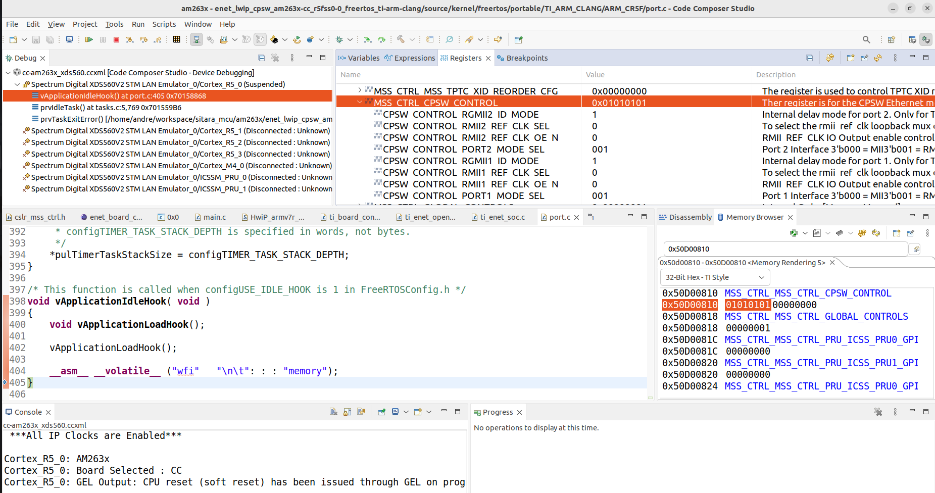
oad program and and verify register MSS_CTRL_CPSW_CONTROL = 0x01010101. This vale is not changed after this API called in all test period.

1.png

2.png

3.png

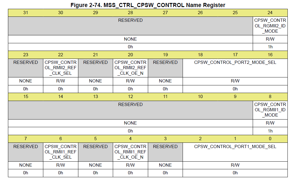
According to TRM, we should be able to generate 50MHz reference clock for RMII1/RMII2.

However, when we measure the signal, RMII1_REF_CLK on R17 pin are missing.

4.png

5.png


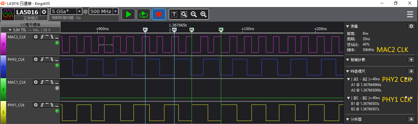
We also set R17 as GPIO and toggle it, we can make sure R17 has correct connection. No layout issue. 

So we would like to know why we can't generate RMII1_REF_CLK? 


Regards

Andre

  • We also found in the ti_pinmux_config.c, there is no pinmux setting for RMII1. It duplicate setting for RMII2. Please check if this is the SDK bug?

    /*
    * Auto generated file
    */
    #include "ti_drivers_config.h"
    #include <drivers/pinmux.h>

    static Pinmux_PerCfg_t gPinMuxMainDomainCfg[] = {
    /* I2C0 pin config */
    /* I2C0_SCL -> I2C0_SCL (A13) */
    {
    PIN_I2C0_SCL,
    ( PIN_MODE(0) | PIN_PULL_DISABLE | PIN_SLEW_RATE_LOW )
    },
    /* I2C0 pin config */
    /* I2C0_SDA -> I2C0_SDA (B13) */
    {
    PIN_I2C0_SDA,
    ( PIN_MODE(0) | PIN_PULL_DISABLE | PIN_SLEW_RATE_LOW )
    },
    /* I2C2 pin config */
    /* I2C2_SCL -> UART0_RTSn (C7) */
    {
    PIN_UART0_RTSN,
    ( PIN_MODE(1) | PIN_PULL_DISABLE | PIN_SLEW_RATE_LOW )
    },
    /* I2C2 pin config */
    /* I2C2_SDA -> UART0_CTSn (B7) */
    {
    PIN_UART0_CTSN,
    ( PIN_MODE(1) | PIN_PULL_DISABLE | PIN_SLEW_RATE_LOW )
    },

    /* MDIO pin config */
    /* MDIO_MDIO -> MDIO_MDIO (N16) */
    {
    PIN_MDIO_MDIO,
    ( PIN_MODE(0) | PIN_PULL_DISABLE | PIN_SLEW_RATE_LOW )
    },
    /* MDIO pin config */
    /* MDIO_MDC -> MDIO_MDC (M17) */
    {
    PIN_MDIO_MDC,
    ( PIN_MODE(0) | PIN_PULL_DISABLE | PIN_SLEW_RATE_LOW )
    },
    /* RMII2 pin config */
    /* RMII2_CRS_DV -> PR0_PRU0_GPIO10 (G18) */
    {
    PIN_PR0_PRU0_GPIO10,
    ( PIN_MODE(2) | PIN_PULL_DISABLE | PIN_SLEW_RATE_LOW )
    },
    /* RMII2 pin config */
    /* RMII2_RXD0 -> PR0_PRU0_GPIO0 (K17) */
    {
    PIN_PR0_PRU0_GPIO0,
    ( PIN_MODE(2) | PIN_PULL_DISABLE | PIN_SLEW_RATE_LOW )
    },
    /* RMII2 pin config */
    /* RMII2_RXD1 -> PR0_PRU0_GPIO1 (K18) */
    {
    PIN_PR0_PRU0_GPIO1,
    ( PIN_MODE(2) | PIN_PULL_DISABLE | PIN_SLEW_RATE_LOW )
    },
    /* RMII2 pin config */
    /* RMII2_RX_ER -> PR0_PRU0_GPIO5 (G17) */
    {
    PIN_PR0_PRU0_GPIO5,
    ( PIN_MODE(2) | PIN_PULL_DISABLE | PIN_SLEW_RATE_LOW )
    },
    /* RMII2 pin config */
    /* RMII2_TXD0 -> PR0_PRU0_GPIO11 (M16) */
    {
    PIN_PR0_PRU0_GPIO11,
    ( PIN_MODE(2) | PIN_PULL_DISABLE | PIN_SLEW_RATE_LOW )
    },
    /* RMII2 pin config */
    /* RMII2_TXD1 -> PR0_PRU0_GPIO12 (M15) */
    {
    PIN_PR0_PRU0_GPIO12,
    ( PIN_MODE(2) | PIN_PULL_DISABLE | PIN_SLEW_RATE_LOW )
    },
    /* RMII2 pin config */
    /* RMII2_TX_EN -> PR0_PRU0_GPIO15 (L16) */
    {
    PIN_PR0_PRU0_GPIO15,
    ( PIN_MODE(2) | PIN_PULL_DISABLE | PIN_SLEW_RATE_LOW )
    },
    /* RMII2 pin config */
    /* RMII2_REF_CLK -> PR0_PRU0_GPIO6 (K15) */
    {
    PIN_PR0_PRU0_GPIO6,
    ( PIN_MODE(2) | PIN_PULL_DISABLE | PIN_SLEW_RATE_LOW )
    },
    /* RMII2 pin config */
    /* RMII2_CRS_DV -> PR0_PRU0_GPIO10 (G18) */
    {
    PIN_PR0_PRU0_GPIO10,
    ( PIN_MODE(2) | PIN_PULL_DISABLE | PIN_SLEW_RATE_LOW )
    },
    /* RMII2 pin config */
    /* RMII2_RXD0 -> PR0_PRU0_GPIO0 (K17) */
    {
    PIN_PR0_PRU0_GPIO0,
    ( PIN_MODE(2) | PIN_PULL_DISABLE | PIN_SLEW_RATE_LOW )
    },
    /* RMII2 pin config */
    /* RMII2_RXD1 -> PR0_PRU0_GPIO1 (K18) */
    {
    PIN_PR0_PRU0_GPIO1,
    ( PIN_MODE(2) | PIN_PULL_DISABLE | PIN_SLEW_RATE_LOW )
    },
    /* RMII2 pin config */
    /* RMII2_RX_ER -> PR0_PRU0_GPIO5 (G17) */
    {
    PIN_PR0_PRU0_GPIO5,
    ( PIN_MODE(2) | PIN_PULL_DISABLE | PIN_SLEW_RATE_LOW )
    },
    /* RMII2 pin config */
    /* RMII2_TXD0 -> PR0_PRU0_GPIO11 (M16) */
    {
    PIN_PR0_PRU0_GPIO11,
    ( PIN_MODE(2) | PIN_PULL_DISABLE | PIN_SLEW_RATE_LOW )
    },
    /* RMII2 pin config */
    /* RMII2_TXD1 -> PR0_PRU0_GPIO12 (M15) */
    {
    PIN_PR0_PRU0_GPIO12,
    ( PIN_MODE(2) | PIN_PULL_DISABLE | PIN_SLEW_RATE_LOW )
    },
    /* RMII2 pin config */
    /* RMII2_TX_EN -> PR0_PRU0_GPIO15 (L16) */
    {
    PIN_PR0_PRU0_GPIO15,
    ( PIN_MODE(2) | PIN_PULL_DISABLE | PIN_SLEW_RATE_LOW )
    },
    /* RMII2 pin config */
    /* RMII2_REF_CLK -> PR0_PRU0_GPIO6 (K15) */
    {
    PIN_PR0_PRU0_GPIO6,
    ( PIN_MODE(2) | PIN_PULL_DISABLE | PIN_SLEW_RATE_LOW )
    },

    /* UART0 pin config */
    /* UART0_RXD -> UART0_RXD (A7) */
    {
    PIN_UART0_RXD,
    ( PIN_MODE(0) | PIN_PULL_DISABLE | PIN_SLEW_RATE_LOW )
    },
    /* UART0 pin config */
    /* UART0_TXD -> UART0_TXD (A6) */
    {
    PIN_UART0_TXD,
    ( PIN_MODE(0) | PIN_PULL_DISABLE | PIN_SLEW_RATE_LOW )
    },

    {PINMUX_END, PINMUX_END}
    };

    Regards

    Andre

  • Hi Andre,

    On our launchpad we have only RGMII and MII phy, so we have not tested RMII before. Our team is looking into this issue. We have tested on other devices, like AM263Px. So we can carry over those fixes here.

  • Nilabh,

       After initial RMII1 pinmux, MAC1 outputs a 50MHz clock.  We need to fix bug in SDK.

    Please provide patch for now. Thanks.

    Regards

    Andre


  • /*
     *  Copyright (C) 2021-2024 Texas Instruments Incorporated
     *
     *  Redistribution and use in source and binary forms, with or without
     *  modification, are permitted provided that the following conditions
     *  are met:
     *
     *    Redistributions of source code must retain the above copyright
     *    notice, this list of conditions and the following disclaimer.
     *
     *    Redistributions in binary form must reproduce the above copyright
     *    notice, this list of conditions and the following disclaimer in the
     *    documentation and/or other materials provided with the
     *    distribution.
     *
     *    Neither the name of Texas Instruments Incorporated nor the names of
     *    its contributors may be used to endorse or promote products derived
     *    from this software without specific prior written permission.
     *
     *  THIS SOFTWARE IS PROVIDED BY THE COPYRIGHT HOLDERS AND CONTRIBUTORS
     *  "AS IS" AND ANY EXPRESS OR IMPLIED WARRANTIES, INCLUDING, BUT NOT
     *  LIMITED TO, THE IMPLIED WARRANTIES OF MERCHANTABILITY AND FITNESS FOR
     *  A PARTICULAR PURPOSE ARE DISCLAIMED. IN NO EVENT SHALL THE COPYRIGHT
     *  OWNER OR CONTRIBUTORS BE LIABLE FOR ANY DIRECT, INDIRECT, INCIDENTAL,
     *  SPECIAL, EXEMPLARY, OR CONSEQUENTIAL DAMAGES (INCLUDING, BUT NOT
     *  LIMITED TO, PROCUREMENT OF SUBSTITUTE GOODS OR SERVICES; LOSS OF USE,
     *  DATA, OR PROFITS; OR BUSINESS INTERRUPTION) HOWEVER CAUSED AND ON ANY
     *  THEORY OF LIABILITY, WHETHER IN CONTRACT, STRICT LIABILITY, OR TORT
     *  (INCLUDING NEGLIGENCE OR OTHERWISE) ARISING IN ANY WAY OUT OF THE USE
     *  OF THIS SOFTWARE, EVEN IF ADVISED OF THE POSSIBILITY OF SUCH DAMAGE.
     */
    
    /*
     * Auto generated file
     */
    #include "ti_drivers_config.h"
    #include <drivers/pinmux.h>
    
    static Pinmux_PerCfg_t gPinMuxMainDomainCfg[] = {
                /* I2C0 pin config */
        /* I2C0_SCL -> I2C0_SCL (A13) */
        {
            PIN_I2C0_SCL,
            ( PIN_MODE(0) | PIN_PULL_DISABLE | PIN_SLEW_RATE_LOW )
        },
        /* I2C0 pin config */
        /* I2C0_SDA -> I2C0_SDA (B13) */
        {
            PIN_I2C0_SDA,
            ( PIN_MODE(0) | PIN_PULL_DISABLE | PIN_SLEW_RATE_LOW )
        },
                /* I2C2 pin config */
        /* I2C2_SCL -> UART0_RTSn (C7) */
        {
            PIN_UART0_RTSN,
            ( PIN_MODE(1) | PIN_PULL_DISABLE | PIN_SLEW_RATE_LOW )
        },
        /* I2C2 pin config */
        /* I2C2_SDA -> UART0_CTSn (B7) */
        {
            PIN_UART0_CTSN,
            ( PIN_MODE(1) | PIN_PULL_DISABLE | PIN_SLEW_RATE_LOW )
        },
    
                /* MDIO pin config */
        /* MDIO_MDIO -> MDIO_MDIO (N16) */
        {
            PIN_MDIO_MDIO,
            ( PIN_MODE(0) | PIN_PULL_DISABLE | PIN_SLEW_RATE_LOW )
        },
        /* MDIO pin config */
        /* MDIO_MDC -> MDIO_MDC (M17) */
        {
            PIN_MDIO_MDC,
            ( PIN_MODE(0) | PIN_PULL_DISABLE | PIN_SLEW_RATE_LOW )
        },
        /* RMII1 pin config */
        /* RMII1_CRS_DV -> PIN_RGMII1_TD2 (P18) */
        {
            PIN_RGMII1_TD2,
            ( PIN_MODE(1) | PIN_PULL_DISABLE | PIN_SLEW_RATE_LOW )
        },
        /* RMII1 pin config */
        /* RMII1_RXD0 -> PIN_RGMII1_RD0 (U17) */
        {
            PIN_RGMII1_RD0,
            ( PIN_MODE(1) | PIN_PULL_DISABLE | PIN_SLEW_RATE_LOW )
        },
        /* RMII1 pin config */
        /* RMII1_RXD1 -> PIN_RGMII1_RD1 (T17) */
        {
            PIN_RGMII1_RD1,
            ( PIN_MODE(1) | PIN_PULL_DISABLE | PIN_SLEW_RATE_LOW )
        },
        /* RMII1 pin config */
        /* RMII1_RX_ER -> PIN_RGMII1_RX_CTL (R18) */
        {
            PIN_RGMII1_RX_CTL,
            ( PIN_MODE(1) | PIN_PULL_DISABLE | PIN_SLEW_RATE_LOW )
        },
        /* RMII1 pin config */
        /* RMII1_TXD0 -> PIN_RGMII1_TD0 (P16) */
        {
            PIN_RGMII1_TD0,
            ( PIN_MODE(1) | PIN_PULL_DISABLE | PIN_SLEW_RATE_LOW )
        },
        /* RMII1 pin config */
        /* RMII1_TXD1 -> PIN_RGMII1_TD1 (P17) */
        {
            PIN_RGMII1_TD1,
            ( PIN_MODE(1) | PIN_PULL_DISABLE | PIN_SLEW_RATE_LOW )
        },
        /* RMII1 pin config */
        /* RMII1_TX_EN -> PIN_RGMII1_TX_CTL (M18) */
        {
            PIN_RGMII1_TX_CTL,
            ( PIN_MODE(1) | PIN_PULL_DISABLE | PIN_SLEW_RATE_LOW )
        },
        /* RMII1 pin config */
        /* RMII1_REF_CLK -> PIN_RGMII1_RXC (R17) */
        {
         PIN_RGMII1_RXC,
            ( PIN_MODE(1) | PIN_PULL_DISABLE | PIN_SLEW_RATE_LOW )
        },
        /* RMII2 pin config */
        /* RMII2_CRS_DV -> PR0_PRU0_GPIO10 (G18) */
        {
            PIN_PR0_PRU0_GPIO10,
            ( PIN_MODE(2) | PIN_PULL_DISABLE | PIN_SLEW_RATE_LOW )
        },
        /* RMII2 pin config */
        /* RMII2_RXD0 -> PR0_PRU0_GPIO0 (K17) */
        {
            PIN_PR0_PRU0_GPIO0,
            ( PIN_MODE(2) | PIN_PULL_DISABLE | PIN_SLEW_RATE_LOW )
        },
        /* RMII2 pin config */
        /* RMII2_RXD1 -> PR0_PRU0_GPIO1 (K18) */
        {
            PIN_PR0_PRU0_GPIO1,
            ( PIN_MODE(2) | PIN_PULL_DISABLE | PIN_SLEW_RATE_LOW )
        },
        /* RMII2 pin config */
        /* RMII2_RX_ER -> PR0_PRU0_GPIO5 (G17) */
        {
            PIN_PR0_PRU0_GPIO5,
            ( PIN_MODE(2) | PIN_PULL_DISABLE | PIN_SLEW_RATE_LOW )
        },
        /* RMII2 pin config */
        /* RMII2_TXD0 -> PR0_PRU0_GPIO11 (M16) */
        {
            PIN_PR0_PRU0_GPIO11,
            ( PIN_MODE(2) | PIN_PULL_DISABLE | PIN_SLEW_RATE_LOW )
        },
        /* RMII2 pin config */
        /* RMII2_TXD1 -> PR0_PRU0_GPIO12 (M15) */
        {
            PIN_PR0_PRU0_GPIO12,
            ( PIN_MODE(2) | PIN_PULL_DISABLE | PIN_SLEW_RATE_LOW )
        },
        /* RMII2 pin config */
        /* RMII2_TX_EN -> PR0_PRU0_GPIO15 (L16) */
        {
            PIN_PR0_PRU0_GPIO15,
            ( PIN_MODE(2) | PIN_PULL_DISABLE | PIN_SLEW_RATE_LOW )
        },
        /* RMII2 pin config */
        /* RMII2_REF_CLK -> PR0_PRU0_GPIO6 (K15) */
        {
            PIN_PR0_PRU0_GPIO6,
            ( PIN_MODE(2) | PIN_PULL_DISABLE | PIN_SLEW_RATE_LOW )
        },
    
                /* UART0 pin config */
        /* UART0_RXD -> UART0_RXD (A7) */
        {
            PIN_UART0_RXD,
            ( PIN_MODE(0) | PIN_PULL_DISABLE | PIN_SLEW_RATE_LOW )
        },
        /* UART0 pin config */
        /* UART0_TXD -> UART0_TXD (A6) */
        {
            PIN_UART0_TXD,
            ( PIN_MODE(0) | PIN_PULL_DISABLE | PIN_SLEW_RATE_LOW )
        },
    
        {PINMUX_END, PINMUX_END}
    };
    
    
    /*
     * Pinmux
     */
    
    
    void Pinmux_init(void)
    {


        Pinmux_config(gPinMuxMainDomainCfg, PINMUX_DOMAIN_ID_MAIN);
        
    }


    Nilabh,

       After initial RMII1 pinmux, MAC1 outputs a 50MHz clock.  We need to fix bug in SDK.

    Please provide patch for now. Thanks.

    Regards

    Andre


  • Hi Andre,

    Pinmux Generation for RMII on AM263x SDK is actual bug. This issue has been fixed with below patch and pinmux generation for RMII is validated. Please use this patch and regenerate ti_pinmux_config.c. This fix will be also available in upcoming AM263X SDK release.

    Patch to fix RMII pinmux generation:

    diff --git a/source/networking/enet/core/sysconfig/networking/.meta/enet_cpsw/am263x/enet_cpsw_am263x_pinmux.syscfg.js b/source/networking/enet/core/sysconfig/networking/.meta/enet_cpsw/am263x/enet_cpsw_am263x_pinmux.syscfg.js
    index 52f8bc1..d6fbc1d 100644
    --- a/source/networking/enet/core/sysconfig/networking/.meta/enet_cpsw/am263x/enet_cpsw_am263x_pinmux.syscfg.js
    +++ b/source/networking/enet/core/sysconfig/networking/.meta/enet_cpsw/am263x/enet_cpsw_am263x_pinmux.syscfg.js
    @@ -206,7 +206,7 @@ function getInterfaceNameList(inst) {
         }
         else if (inst.phyToMacInterfaceMode === "RMII")
         {
    -        interfaceNameList.push(getInterfaceName(inst, "RMII2"));
    +        interfaceNameList.push(getInterfaceName(inst, "RMII1"));
             interfaceNameList.push(getInterfaceName(inst, "RMII2"));
         }
         else


    I am currently analyzing 'MSS_CTRL_CPSW_CONTROL' register issue mentioned above for RMII mode in AM263x. I will update here in sometime regarding this issue.

    Regards,
    Ranga Rakesh

  • Ranga, 

         We already get RMMI1_REF_CLK 50MHz after fixing pinmux problem.

    Regards

    Andre