This thread has been locked.

If you have a related question, please click the "Ask a related question" button in the top right corner. The newly created question will be automatically linked to this question.

AM2431: Question about PRU IO Control delay

Part Number: AM2431

Hi experts,

When using the PRU for reading and writing I/O, we noticed a potential delay. Please help confirm whether this issue exists and if there are any methods to resolve it.

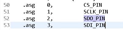
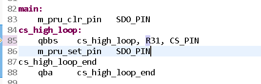
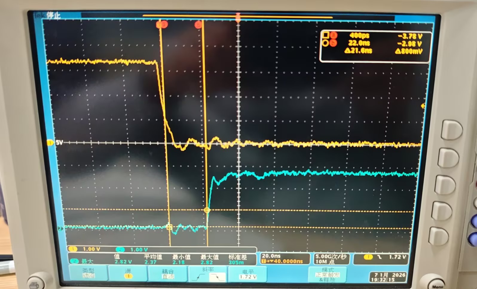
Using the PRU as an SPI slave, after detecting the falling edge of CS, we pull SDO high. The code only consists of two instructions, but the SDO level rises 21 ns later. Current testing indicates that the detection of the CS pin is delayed, as if there is a latency in the GPIO input pin.

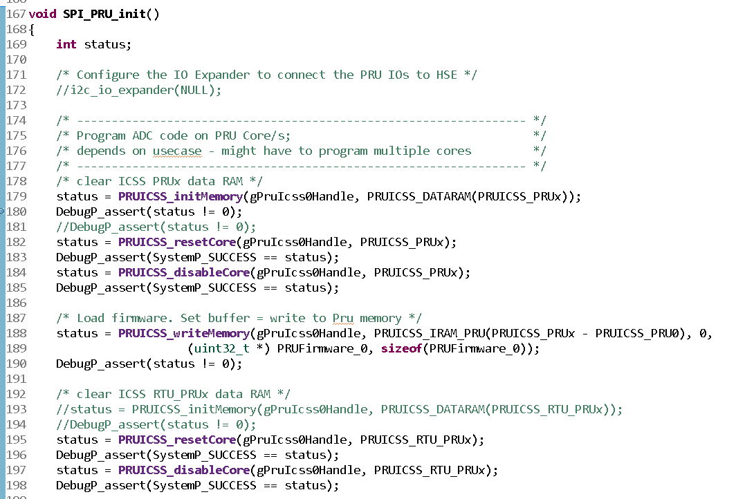
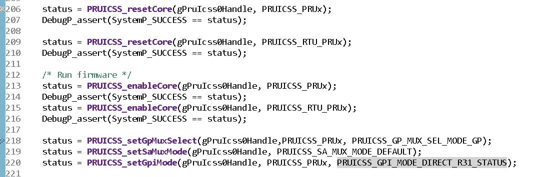
Below are the test code and waveforms.

0.0.png

0.1.png

1.0.png

2.0.png

2.1.png

2.2.png

4.jpg

  • Hello,

    Please share the macro that you are using to set the signal.

    I would expect 2 PRU clock signals for the signal to get from the processor pin into the R31, and about 2 clock signals for the write to R30 to be observable on the processor pin (3ns each clock cycle if running at 333MHz). That plus the time to execute the 2 instructions Back on AM335x, I tested with a simple loopback wire from the GPO pin to the GPI pin, and observed 6 clock cycles total to write, read, and execute the instructions (5ns/clock). A longer loopback wire added additional clock cycles since it took the electrons longer to travel. When I tested on AM64x EVM with much longer traces in the PCB, I think I saw 7 clock cycles for the same test (3ns/clock).

    Regards,

    Nick

  • Hi Nick,

    Please double check my response, the CS_PIN is from SPI master, it was falling edge, it SHOULD be detected by PRU GPI within maximum 2 instructions, so it SHOULD be 6ns(3ns/clock) not 21ns.

    Thanks

    Kelven

  • Hi Nick,

    The set pin macro is from TI, please see the below

    m_pru_set_pin    .macro PRU_PIN

       set        r30,    r30,    PRU_PIN

    .endm

    The set signal is just 1 instruction, so for CS_PIN detection, it SHOULD be within 2 instructions, the SDO_PIN will be rising within 2+1 = 9ns.

    Thanks

    Kelven

  • I would expect 2 PRU clock signals for the signal to get from the processor pin into the R31, and about 2 clock signals for the write to R30 to be observable on the processor pin (3ns each clock cycle if running at 333MHz).

    Do you mean the delay on the path between pad and R30/R31 is 2 clock? what is the clock unit? it should not be PRU clock on the path.

    I made a timing diagram to help understand the delay of the code, is it correct?

    The delay is a very important characteristic when evaluate its capability. it will be good to record down.

  • The assembly program purpose was:
    When detect CS_PIN was low, the SDO_PIN will be output as high level, the CS_PIN was from external SPI master device, the CS_PIN low signal detection will be within maximum 2 instructions(3ns/clock), so the maximum detction time SHOULD be 2*3ns = 6ns, the SDO_PIN output will be 1 instruction, the total time SHOULD be 6ns+3ns = 9ns not 21ns as the below picture showed.

    ...

  • Hi Kelven,

      3 cycle latency is the digital delay coming from PRU instructions. There is additional analog delay from IO pads, PCB, connector. Especially the IO pad has for example a mux to select different pin modes, schmitt trigger option and debounce logic. You can check whether schmitt tigger and debounce logic is disabled to get min delay. However, the fact that you can select various options on IO pad means there is a fixed delay. 

    TRM chapter "5.1.1.3 CTRL_MMR0 and PADCFG_CTRL0_CFG0 Functional Description" has the details on the pad settings. 

    So we can only confirm that 18 + 3 ns latency is the best you can get with this implementation. Does this cause a problem in your application? What is the maximum delay between CS and SDO you are looking for?

    - Thomas

  • Hi Thomas,

    Thank you for your confirmation.

    Please double check the above waveform:

    Step 1. When detect CS_PIN falling edge, the SDO_PIN will output low level ahead of SPI_CLK, the latency is 21ns, it is confirmed;

    Step 2. When detect 1st SPI_CLK rising edge, the SDO_PIN will keep low level; here if the SDO_PIN was kept with low level, but the latency was still existing, it was also 21ns, please confirm???

    Step 3. When detect 2nd SPI_CLK rising edge, the SPO_PIN will output high level, was the latency still existing? It was 21ns, please confirm??? 

    Shortly summarized: The 21ns latency is always existing on SPI_CLK rising edge detection + SDO_PIN output no matter what the SPI_CLK rising edge is 1st or 2nd or 3rd......

    Please help to double confirm the point.

    Thanks

    Kelven

  • Hi Thomas,

    Thank you for your confirmation.

    Please double check the above waveform:

    Step 1. When detect CS_PIN falling edge, the SDO_PIN will output low level ahead of SPI_CLK, the latency is 21ns, it is confirmed;

    Step 2. When detect 1st SPI_CLK rising edge, the SDO_PIN will keep low level; here if the SDO_PIN was kept with low level, but the latency was still existing, it was also 21ns, please confirm???

    Step 3. When detect 2nd SPI_CLK rising edge, the SPO_PIN will output high level, was the latency still existing? It was 21ns, please confirm??? 

    Shortly summarized: The 21ns latency is always existing on SPI_CLK rising edge detection + SDO_PIN output no matter what the SPI_CLK rising edge is 1st or 2nd or 3rd......

    Could you please help to double confirm this point? The 21ns latency for SPI_CLK rising edge detection+SDO_PIN output is always existing on each of SPI_CLK.

    Thanks

    Kelven

  • Hi Kelven,

      in case of SPI peripheral mode (external CS and CLK) the default case is as you describe above - 21 ns. Note on my measurement it is 18 ns fixed delay and 3 ns jitter coming from async clock sources - external clock running from different oscillator compared to AM243x. Only in case you use same clock reference for AM243x and external SPI device, then there will be no jitter of 3 ns. 

    If external SPI device has fixed timing for CS and CLK we can optimize latency on SDO. Use CS as reference for first SDO and use previous clock edge for following CLK to SDO. 

    - Thomas

  • Hi Thomas,

    Thank for your support.

    Yes, we had designed our SPI slave device just like you proposed, the SPI slave device works fine.

    Thanks 

    Kelven

  • I am doing a deep dive into the circuit design to make sure that I understand the signal path for both R30 & R31 (i.e., try to isolate what is IO/PCB latency, and what is latency for getting between R30/R31 and the pins).

    There is definitely a single flop on the input path (PCB -> IO -> flop -> pru.r31). So I think it would look like this, but I am verifying with the design team:
    Clock 1: signal latched into the flop (the signal goes from async to sync clock sources as Thomas said)
    Clock 2: signal latched into r31
    Clock 3: QBBS recognizes the change to r31

    Please ping the thread if I have not replied by Friday.

    Regards,

    Nick

  • Thank you Nick for your feedback.

  • Hi,

    The thread owner is out of office till until week of Feb 17. Please ping the thread if you do not get an update during that week.

    Thank you for your patience.

    Regards,
    Harshith

  • Hi Nick, 

    Is there update? maybe this input path delay data can help the other topic in discussing:

     RE: AM2432: SPI peripheral mode switching characteristics 

  • Hello Tony,

    Thanks for the ping, I started replying to this a few weeks ago and then lost my draft.

    I drew a graphic for this, and now... it seems like I am unable to copy/paste images into e2e replies. I will email the graphics to you, feel free to ping me again in a few days when e2e allows us to copy/paste images into the responses again. Or you could respond to the e2e with the images I sent you.

    Text explanation

    If we want to read in a signal and then drive an output signal based on the input:

    5 PRU clock transitions need to occur from the moment the input signal is latched into an input flop within the PRU subsystem, to the moment that the output signal is driven from the output flop. This is the fixed time in the PRU's synchronous clock domain: 15 ns at 3ns/clock, up to 25 ns at 5 ns/clock, depending on the PRU's clock frequency.

    You still need to take PCB trace latency into account, as well as the additional latency that it takes for the signal to pass through the asynchronous logic between the PRU's flops and the processor's pins. I was told that a few nanoseconds of additional latency is to be expected.

    When you add up both sources of latency, latency of 18-21 ns for you to measure sending a signal from somewhere else on your PCB, and waiting to see a response signal, is absolutely reasonable.

    Regards,

    Nick

  • Here are the diagrams from earlier:

    Takeaway: We spend 5 PRU clocks in the PRU’s synchronous time domain (15 ns if PRU core is running at 3ns). Additional latency comes from asynchronous logic outside of the PRU subsystem. I have not spent time experimenting with Thomas’s suggestions around disabling schmitt trigger and debounce logic to potentially reduce that time spent in the asynchronous logic, so I am not sure whether 1) these settings are enabled by default, and 2) if you ran tests with the settings enabled, and then disabled them, whether the improvement would be large enough to measure.