This thread has been locked.

If you have a related question, please click the "Ask a related question" button in the top right corner. The newly created question will be automatically linked to this question.

MSPM0L1227: How to set Flash Memory Static Write Protection (SWP)

Part Number: MSPM0L1227
Other Parts Discussed in Thread: SYSCONFIG, LP-MSPM0L2228,

Hi,

My customer has a question about the specification of Flash Memory Stack Write Protection (SWP).


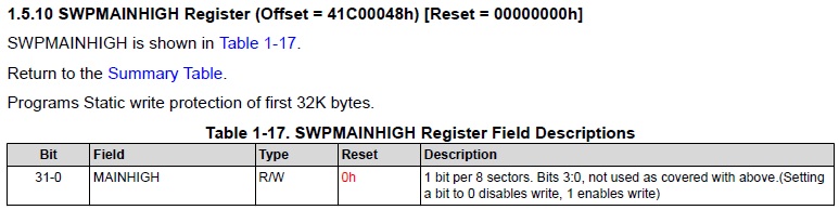
According to the TRM, it seems that the first 32Kbyte can be set as SWP by one sector, and the other can be set by eight sectors.

They wanted to use this function to disable SWP only for certain sectors of Flash Memory on Sysconfig in CCS and enable other regions in order to internally rewrite in the SWP disabled area even after writing ROM.

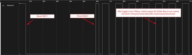
However, this operation failed to write the SWP disabled area, and the operation did not work as intended.

Could you please let them know if there is a wrong recognition or usage of this feature.


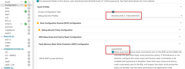
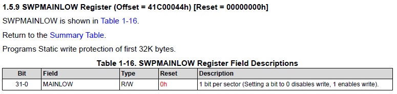
From the description of SWP Register in TRM

SWPMAINLOW.jpg


SWPMAINHIGH.jpg


The Screen of SysConfig

Sysconfig>Software>Configuration NVM>SWP Configuration CCS

SWP.jpg

They set the sector 0 to 3 : bit[3:0] in the first 32Kbyte as “1” (Disabling protection), and the sector 4 to 31 : bit[31:4] are set as “0” (Enabling Protection).


Thanks and regards,

Hideaki

  • Hi Hideaki,

    They set the sector 0 to 3 : bit[3:0] in the first 32Kbyte as “1” (Disabling protection), and the sector 4 to 31 : bit[31:4] are set as “0” (Enabling Protection).

    This looks fine to me. So, what does customer finding according to this setting? 

    The flash loader or application code can not write or erase 5KB-32KB address anymore.

    Note that the NONMAIN setting need MCU reset or repower to take effect.

    Another guess is that does they successfully download NONMAIN to the device?

    B.R.

    Sal

  • Hi Sal,

    Thank you for your comment and sorry for my late response.

    Note that the NONMAIN setting need MCU reset or repower to take effect.

    Another guess is that does they successfully download NONMAIN to the device?


    They write the firmware to the MSPM0L1227 device on their board by using the on-board emulator on the LP-MSPM0L2228.

    At that time, it was written to NONMAIN and finished correctly and it is working, so they think there is no problem with the above two.


    What they want to do is to write/log to the Flash area where has not been set as SWP for counting the number of boot times after writing firmware to the device. However, it fails.

    The program area is SWP enabled and the rewritable free area is SWP disabled.

    Please let them know if there is any problem on their procedure.

    Or it would be appreciated if you could tell them what functions SWP is supposed to be used for, if their use case is wrong.


    Thanks and regards,

    Hideaki

  • Hideaki,

    There has a document for NONMAIN User Guide: MSPM0 NONMAIN Flash Memory Configuration Guide

    What they want to do is to write/log to the Flash area where has not been set as SWP for counting the number of boot times after writing firmware to the device. However, it fails.

    According to the configuration, 0-4KB can be write. What the issues they found, any screenshot on their code or failure phenomenon?

    For FLASH operation, follow the SDK example:

    dev.ti.com/.../node

    B.R.

    Sal

  • Hi Sal,

    Thank you for your reply, but let me confirm. Why do you mention about NONMAIN Flash ?

    Unfortunately, they cannot get a screenshot, because MSPM0L1227 is running on stand-alone and the debug is disabled.

    Thanks and regards,

    Hideaki

  • Hi Sal,

    The customer was able to confirm that SWP works as they expected.

    They found that the difference was the setting of the Debug Security Profiles.

    When they set the Debug Security Profiles as “Security Level 2” to be disable the debug port, SWP doesn’t work correctly as mentioned above.


    Is there a possibility that there will be badl effects if multiple security functions are set at the same time?

    They want to set as "Security Level 2". Is it possible ? How can they solve this issue ?

    Thanks and regards,

    Hideaki 

  • Hi Hideaki,

    I think this should not effect.

    While I haven't test this before. Let me do some experiment with this configuration and get back to you.

    B.R.

    Sal

  • Hi Hideaki,

    After test with L2228, the Security Level 2 does not impact SWP function.

    The sysconfig setting:

    It protect 4-8KB flash range in SWP of NONMAIN (NVM).

    The test code:

    #include "ti_msp_dl_config.h"
    /* Base address of test main memory */
    #define NONMAIN_BASE_ADDRESS                                      (0x00001000U) //4-5KB
    
    __attribute__((used, persistent, location(0x1000))) unsigned int dataFlash_1 = 0x12345678;
    __attribute__((used, persistent, location(0x1004))) unsigned int dataFlash_2 = 0x9ABCDEF0;
    
    int main(void)
    {
        volatile DL_FLASHCTL_COMMAND_STATUS gFlashStatus;
        volatile uint32_t gFlashData;
    
        SYSCFG_DL_init();
    
        delay_cycles(32000000*5);   // delay 5s
    
        /* Clear STATCMD register, unprotect MAIN, and then erase MAIN memory */
        DL_FlashCTL_executeClearStatus(FLASHCTL);
        DL_FlashCTL_unprotectSector(
            FLASHCTL, NONMAIN_BASE_ADDRESS, DL_FLASHCTL_REGION_SELECT_MAIN);
        gFlashStatus = DL_FlashCTL_eraseMemoryFromRAM(
            FLASHCTL, NONMAIN_BASE_ADDRESS, DL_FLASHCTL_COMMAND_SIZE_SECTOR);
    
        if(gFlashStatus == DL_FLASHCTL_COMMAND_STATUS_FAILED) {
            delay_cycles(8000000);
            DL_GPIO_togglePins(GPIO_LEDS_PORT, GPIO_LEDS_USER_LED_1_PIN);
            delay_cycles(8000000);
            DL_GPIO_togglePins(GPIO_LEDS_PORT, GPIO_LEDS_USER_LED_1_PIN);
            delay_cycles(8000000);
            DL_GPIO_togglePins(GPIO_LEDS_PORT, GPIO_LEDS_USER_LED_1_PIN);
            /* Lighting LED with 0.25s */
        }
    
        gFlashData = *(uint32_t*)(0x1000);
    
        if(gFlashData == 0x12345678) {
            while(1){
                delay_cycles(16000000);
                DL_GPIO_togglePins(GPIO_LEDS_PORT, GPIO_LEDS_USER_LED_1_PIN);
            }
        }
    
        while (1) {
            delay_cycles(32000000);
            DL_GPIO_togglePins(GPIO_LEDS_PORT, GPIO_LEDS_USER_LED_1_PIN);
        }
    }

    The test result:

    B,R,

    Sal