MSPM0G3519: SPI Configuration for DRV8363S

Part Number: MSPM0G3519
Other Parts Discussed in Thread: DRV8363, SYSCONFIG

Hi,

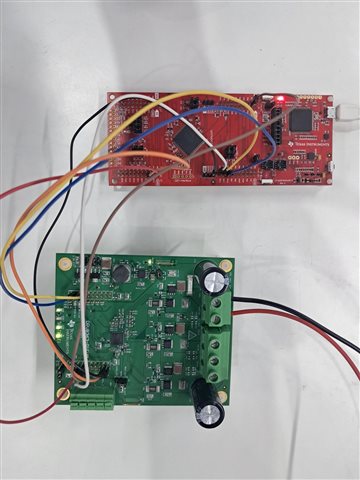
I am working on MSPM0G3519 and DRV8363S.
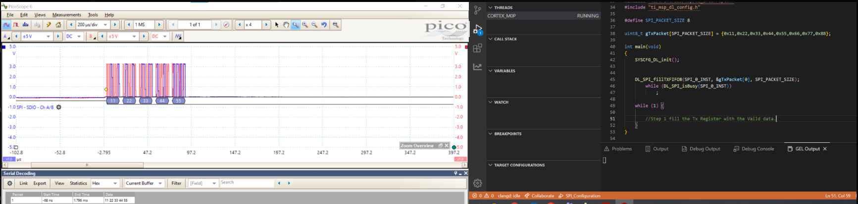
I started with basic SPI peripheral initialization to verify data sent from PICO.
I sent 0x11, 0x22, 0x33, 0x44, 0x55, 0x66, 0x77, 0x88 but only received
0x11, 0x22, 0x33, 0x44, 0x55. Also, I have verified that the return value from the function DL_SPI_fillTXFIFO8 is 5. 


Why are only 5 bytes transmitted?

image.png

image.png


image.png

Regards,

Sakhan

  • I have used the 

    DL_SPI_transmitDataBlocking8 function to send the 8 bytes of data and I got the same in the picoscope. What is the difference in both function?

  • I could not find the thread, but I believe that this is due to the FIFO. You can only send 5 bytes (1 immediate and 4 in the FIFO) before you have to wait for the FIFO to clear to send the next batch. Why the 8 byte transmit fails, I have no idea.

  • The SPI TX FIFO is only 4 entries [Ref TRM (SLAU846C) Sec 25.2.2.5].

    You get the "extra" (5th) entry since as soon as the FIFO goes non-empty it pops the first entry into the FIFO Shift Register.

    DL_SPI_transmitDataBlocking8() waits for the transmission to complete After loading the FIFO, so there's never more than 1 entry there.

    [Edit: Fixed goof.]

  • Hi Bruce and Keith,

    I have configured the MSPM0 SPI controller to send the DRV8363 SPI frames.

    IC_STAT1 Register (Offset = 0h) [Reset = 8080h]

    Now Address of IC_STAT1 Register is 0x00 (Offset = 0h).

    RW is 1

    Data is 0x0000 

    Parity is 1

    1. The frame formed as per the DRV SDI Frame format (24 bits). Verified the SPI Tx and Rx by Enabling the Internal Loop Mode before connecting to DRV8363.

    2. Code Section

    #include "SPI_Frames.h"
    #include "globalVariables.h"
    #include "ti_msp_dl_config.h"
    #include <ti/driverlib/m0p/dl_interrupt.h>
    
    #define SPI_PACKET_SIZE 8
    #define TIME_BETWEEN_EACH_FRAME 13 // 400ns is 13, 1us is 32 (as per DRV datasheet)
    
    SDI_Frame tx;
    SDO_Frame rxFrame;
    uint8_t gTxPacket[SPI_PACKET_SIZE] = {0x11, 0x22, 0x33, 0x44,
                                          0x55, 0x66, 0x77, 0x88};
    uint32_t sendBytes;
    uint8_t i;
    uint8_t sdi[3];
    uint8_t txBytes[3];
    uint8_t rxBytes[3];
    
    //func proto
    static SDO_Frame drv8363_spi_transfer_frame(SDI_Frame txFrame);
    
    int main(void) {
      SYSCFG_DL_init();
    
      //nSLEEP to "HIGH" (Enable the DRV)
      DL_GPIO_setPins(GPIO_GRP_0_PORT, GPIO_GRP_0_PIN_B12_PIN);
      drv8363_ReadFrame(&tx, 0x00);
      
    
        drv8363_spi_transfer_frame(tx);
    
        drv8363_ReadFrame(&tx, 0x00);
        
        drv8363_spi_transfer_frame(tx);
    
      while (1) {
      }
    }
    
    static SDO_Frame drv8363_spi_transfer_frame(SDI_Frame txFrame)
    {


        /* -------- Split SDI raw into 3 bytes (MSB first) -------- */
        txBytes[0] = (txFrame.raw >> 16) & 0xFF;
        txBytes[1] = (txFrame.raw >> 8)  & 0xFF;
        txBytes[2] = (txFrame.raw)       & 0xFF;
    
        /* -------- Start SPI frame -------- */
         for (int i = 0; i < 3; i++)
        {
            DL_SPI_transmitDataBlocking8(SPI_0_INST, txBytes[i]);
            rxBytes[i] = DL_SPI_receiveDataBlocking8(SPI_0_INST);
        }
    
        while (DL_SPI_isBusy(SPI_0_INST));
    
        /* -------- End SPI frame -------- */
    
    
        /* -------- Assemble received bytes into SDO raw -------- */
        rxFrame.raw =
            ((uint32_t)rxBytes[0] << 16) |
            ((uint32_t)rxBytes[1] << 8)  |
            ((uint32_t)rxBytes[2]);
    
        return rxFrame;
    }


    3. Verified the PICO pin data using the Picoscope. There are 48 rising edge (Each frame = 24 clock rising edge) 

    4. Now, connected the DRV8363 with proper pin mapping. [SPI CLK to DRV SCLK, SPI CS to nSCS, SPI PICO to SDI, SPI POCI to SDO]

    Also, the nSLEEP made HIGH to clear Fault Pin after power up. Refer the below MSPM0 and DRV setup,

    When I send the read frame [0x810000] to DRV there is no response (nothing recieved in Rx register) why? Even I achieved delay between each frame sent to MSPM0 to DRV (Refer the Picoscope data).

    I am not getting the data from the DRV even after sending required frames? 

    Kindly help me on this.

    Regards,

    SaKhan

  • Mode "Motorola 4-wire" implies a hardware /CS (PC7 in your case). The SPI unit will de-assert nSCS between bytes if either (a) SPH=0 or (b) the TX FIFO goes empty [Ref TRM (SLAU846C) Sec 25.2.3.1]. While DRV8363 datasheet (SLVSHQ3) Sec 6.6.1 doesn't say it explicitly, it suggests that nSCS has to stay asserted for all 3 (or 4 with CRC) bytes. In general: You should use a GPIO for nSCS (you can use PC7 if you want) rather than the hardware /CS.

    --------------

    To get you going right now: It appears that you're using SPH=1 ("captured on second clock edge"), which keeps /CS asserted over a "continuous back-to-back" sequence of bytes, meaning "the TX FIFO never goes empty". You can (usually) accomplish this by pre-loading the TX FIFO. As near as I can tell, DRV8363 transactions are all 3-byte (or 4-byte with CRC), which Will fit in the FIFO.

    So I suggest you go back to using DL_SPI_fillTXFIFO8() but limit yourself to 3 (or 4) bytes at a time. [Even this is not guaranteed, so long-term you should consider using a GPIO for /CS.]

  • Hi Bruce,

    I have made the suggested changes 4  wire to 3 wire (Manuall CS). Now my CS is continuosly LOW for whole SPI Frame ( No de-assert).

    Then I have used the TXFIFO instead of TXBlocking, I have observed the full 24 clock cycles as expected.

    1. But there is no response from the DRV after send the exact frame from the MSPM0G3519. Could you please confirm the below send and receive function implementation correct?

    2. Is any implemented library available for DRV8363 (any other TI MCU instead of MSPM0G3519 also fine). 

    Regards,

    SaKhan

  • 1A) I don't see anything obviously wrong with your code. Maybe check your wiring (again)?

    1B) Supposing that the lower trace is /CS, I notice that it's low (asserted) until just before the transaction starts, and very briefly goes high before going low again for the transfer. At 1Msps I can't tell how long it is, but data sheet (SLVSHQ3) Sec 5.6 requires it to be high for at least ~0.5usec. I suggest you set your /CS pin initially =1 (I think Sysconfig can do this) which should assure /CS idles high even at startup.

    2) Truth be known, I don't know much about this device (but I have done some SPI in my life). The EVM page (here) offers a downloadable sample (DRV8363_Sensored_Trap.zip) which contains source for the F28 (Piccolo), and there is an spi_read() function which (I think) does pretty much what you're doing. [Though I don't quite understand why it dummy-reads SPIRXBUF immediately after each SPITXBUF write.]