MSPM0L1227-Q1: Customer couldn't flash the program with debugger after enabling Bank Swap.

Part Number: MSPM0L1227-Q1
Other Parts Discussed in Thread: UNIFLASH

Hi Experts.

Our customer faced the issue that they couldn't flash the program with debugger after enabling Bank Swap. They would like to know the reason why this behavior happen. Could you answer following 3 questions.

  1. Does this behavior happens even they use UniFlash?
  2. Could you tell them why this behavior happen?
  3. How to resolve this issue?

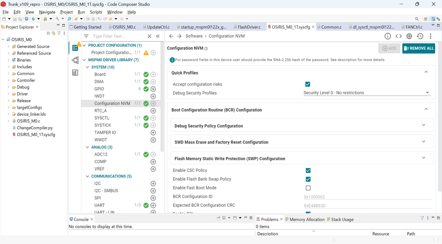
Here is configration of Sysfg.

image.png

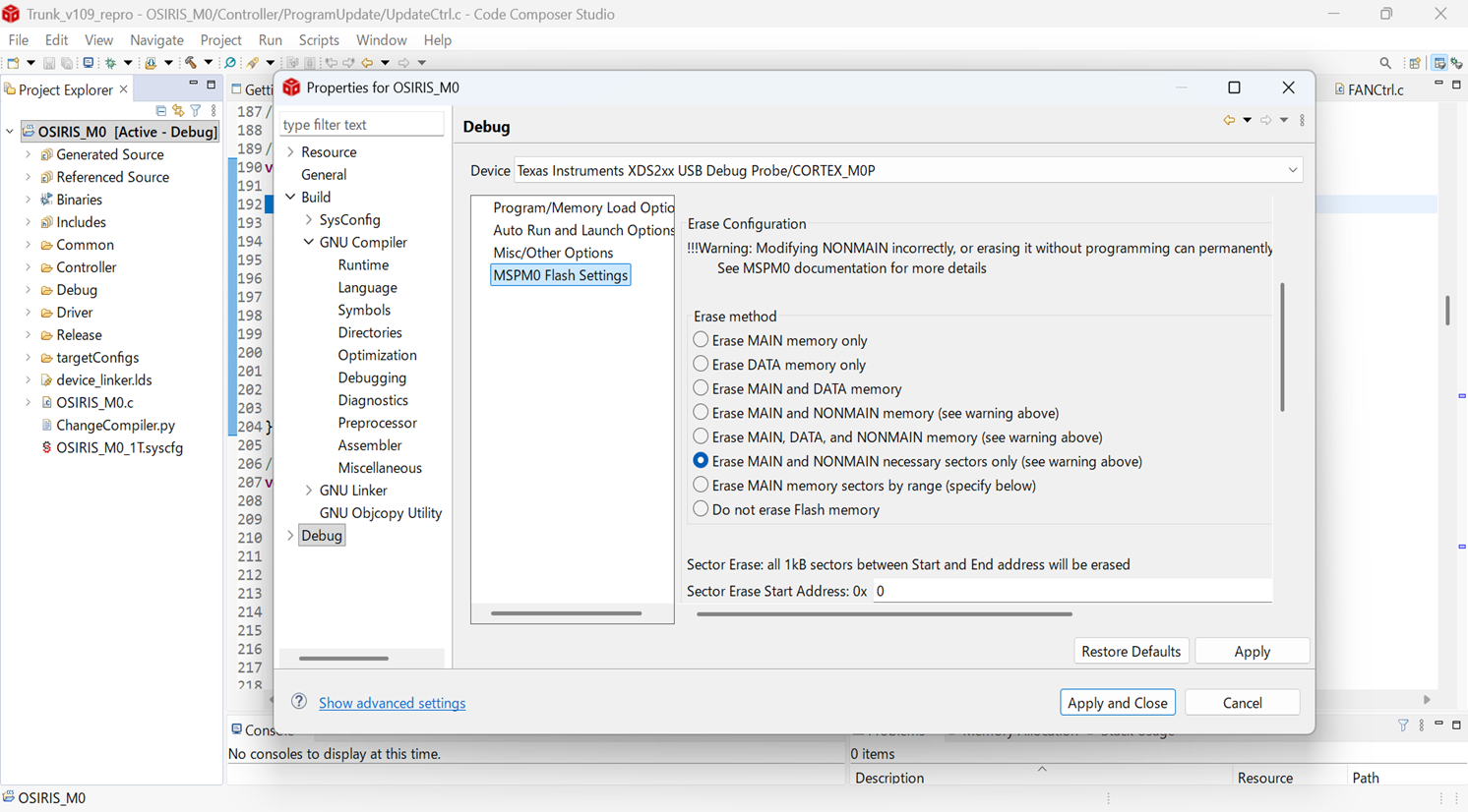
Configration for debuging.

image.png

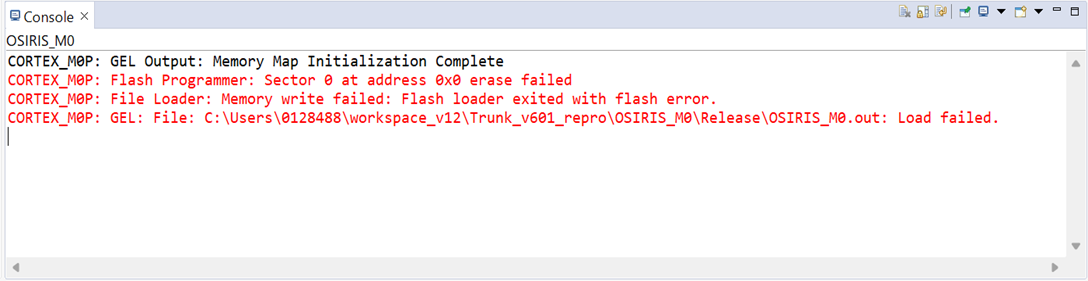
Following error happens during the loading the out file after executed Bank Swap(Current Bank is 1).

Register value.

image.png

Log

image.png

Best regards,

Ito

(b35ef7ae-5bef-4ff2-ac3a-4d8fad4c5e31)

  • Hi Ito,

    It looks like that when bank swap is enabled, the logic bank 0 is auto write protected, and if you are trying to program (by Uniflash or CCS) MCU for address 0x00000-0x10000 (logic bank 0), it will show erase error due to logic bank 0 is protected.

    There are two ways for this situation:

    1. If only the application firmware need to be updated, then the firmware could be updated to 0x10000 - 0x20000 (logic bank 1) address, it should work.

    2. If the boot program also need to be updated, then customer needs to take a factory reset firstly and then program the boot firmware.

    Best Regards,

    Pengfei

  • Hi Pengfei,

    Thank you very much for your feedback.

    We understood there was one method to flash the firmware (bank 0) during the logic bank 0 is protected. But customer mentioned that they need to modify the board if this case happen.

    Do you have any other idea to erase bank 0 when the logic bank 0 is protected? If there is another method, it is really helpful for them.

    Best regards,

    Ito

  • Hi Ito,

    As I mentioned in #2, the factory reset shown in Unlock MCU of MSPM0 MCUs Development Guide (Rev. G) could always be a way to erase the whole MCU to its factory states, and then re-program new firmware to device.

    Best Regards,

    Pengfei

  • Hi Pengfei,

    Thank you for your advice.

    Customer doesn't have JTAG(SWCLK, SWDIO) on customer's board. So I mentioned that they need to modify their board. I'm sorry for your confusion.

    Best regards,

    Ito

  • Hi Ito,

    Oh, so how does customer program their firmware to MCU for the first time?

    They could also connect those SWD pins out if there is any test points for them.

    But I think the below error log should occur when they try to update firmware for address range 0x0000-0x10000 by XDS110 and SWD, right?

    image.png

    Best Regards,

    Pengfei

  • Hi Pengfei,

    I'm sorry for your confusion. I'll confirm.

    Best regards,

    Ito

  • Hi Pengfei,

    I confirmed that they are using SWCLK, SWDIO for flashing. But there is no NRST for factory reset on their board.

    The situation when customer needs to flash after bank swap is limited. So they will modify the board to extend NRST line on a few boards.

    Thanks a lots. Please close this thread.

    Best regards,

    Ito