This thread has been locked.

If you have a related question, please click the "Ask a related question" button in the top right corner. The newly created question will be automatically linked to this question.

AM3358: Signal drift when reading with ADC

Part Number: AM3358

(This is related to a prior inquiry and I think I have linked to it but the update system didn't make it clear that I did.) I have different questions this time.
For background, this sensor is being read with a BeagleBone Black under Linux with  C code using pru0.   Our problem is still that we get a 10-30mv drift up on the signal when the ADC steps are enabled.  I will post our code below but here is the simple sensor circuit first.   

Simple sensor circuit.png

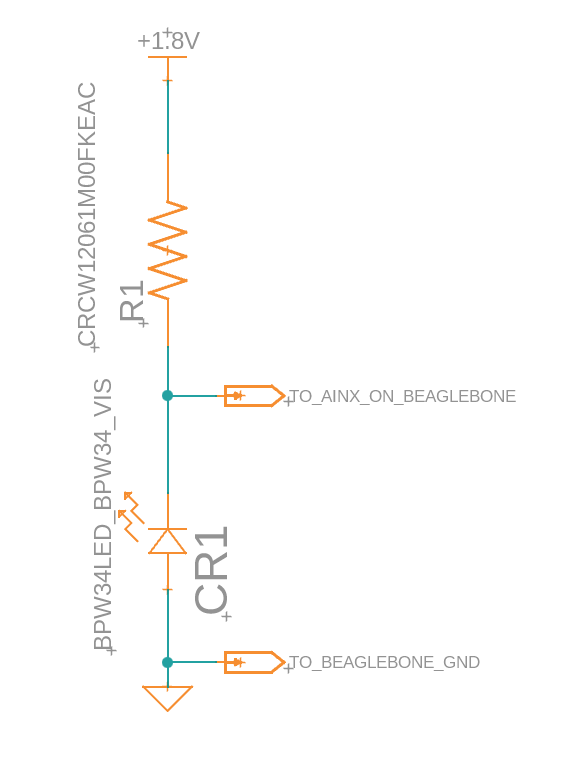
Basically, when light strikes CR1, the voltage output at TO_AINx)... approaches zero.  When the light is blocked, the voltage output at TO_AINx rises toward 1.6V.  This circuit is fundamental to our system and has worked very well for our application.  Changing it is not currently an option.

The issue is that when we monitor TO_AINx through a unity-gain voltage follower and on a scope, the signal is near zero (e.g., 5 mV) when light is striking CR1, until we start reading the signal with the AM3558's ADC using the BeagleBone.   Then, the signal drifts up anywhere from 10-30mv.

The signal currently goes into AIN0 on the ADC.  We also use AIN5 as the second step to read another sensor.  We have just two steps enabled.   They are in one-shot mode.  Again, I'll post the set up code below.

I have had a few suggestions about this and would like input from TI before making changes please.

1) It has been suggested that AIN5-AIN7 have less potential to do this because of how they are charge coupled.  We can try using AIN6 without too much of a hack on the board.  (But this signal would pass through a unity-gain voltage follower circuit mentioned above, combining the two changes.)


a) Is this suggestion valid?

b) If it is valid, must I cut the connection to AIN0 to eliminate the current effect even it I disable AIN0?

2) It has been suggested that all unused AIN inputs be tied to ground. Is there value in this toward solving this problem?

3) Are there any configuration options for the channels that would reduce the drift problem?   We currently read the input in a loop as fast as we can.

4) The signal in to AIN5 does not appear to have this drift problem.  However, in this case, the signal is coming through an op amp on the output stage of a custom current loop to analog converter.  This, in my thinking, lends credence to the idea that there may be a leakage current on the section that has the drift.

Here are the two PRU code routines involved.

static void ADCConfigure(void)
{
	unsigned int i, count, data;
// // Actual sensor name as been replaced with "SENSOR WITH DRIFT" to mask a bit of our proprietary process.
	/* Enable ADC module clock */
	HWREG(SOC_CM_WKUP_REGS + CM_WKUP_ADC_TSC_CLKCTRL) = 0x02;

	/* Disable ADC module for configuration */
	HWREG(SOC_ADC_TSC_0_REGS + TSC_ADC_SS_CTRL) &= ~0x01;

	/* fs = 24MHz / ((CLKDIV+1)*2*Channels*(OpenDly+Average*(14+SampleDly)))
	 *    = 53.57kHz
	 * CLKDIV = 0
	 * Channels = 1
	 * Average = 16
	 * OpenDly = 0
	 * SampleDly = 0
	 */
	HWREG(SOC_ADC_TSC_0_REGS + TSC_ADC_SS_ADC_CLKDIV) = 0;

	HWREG(SOC_ADC_TSC_0_REGS + TSC_ADC_SS_ADCRANGE) = 0xFFF << 16;

	/* Disable all steps for now */
	HWREG(SOC_ADC_TSC_0_REGS + TSC_ADC_SS_STEPENABLE) &= 0xFF;

	/* Unlock step configuration */
	HWREG(SOC_ADC_TSC_0_REGS + TSC_ADC_SS_CTRL) |= 0x04;


	//Step 0 config: SW mode, one shot mode, fifo 0, channel 0, AIN0 on the Beaglebone Black, 4 samples averaged
	//SENSOR WITH DRIFT
	HWREG(SOC_ADC_TSC_0_REGS + TSC_ADC_SS_STEPCONFIG(0)) = 0x00000008;
	
	//Step 1 config: SW mode, one shot mode, fifo 0, channel 1, AIN1 on the Beaglebone Black, 4 samples averaged
	//FLOW METER
//	HWREG(SOC_ADC_TSC_0_REGS + TSC_ADC_SS_STEPCONFIG(1)) = 0x00080000; //no averaging
//	HWREG(SOC_ADC_TSC_0_REGS + TSC_ADC_SS_STEPCONFIG(1)) = 0x00080004; //averages 2 samples
	HWREG(SOC_ADC_TSC_0_REGS + TSC_ADC_SS_STEPCONFIG(1)) = 0x00080008; //averages 4 samples
//	HWREG(SOC_ADC_TSC_0_REGS + TSC_ADC_SS_STEPCONFIG(1)) = 0x0008000C; //averages 8 samples	
//	HWREG(SOC_ADC_TSC_0_REGS + TSC_ADC_SS_STEPCONFIG(1)) = 0x00080010; //averages 16 samples	
	
	//Step 2 config: SW mode, one shot mode, fifo 0, channel 4, AIN4 on the Beaglebone Black, 4 samples averaged
	//UNUSED
	//HWREG(SOC_ADC_TSC_0_REGS + TSC_ADC_SS_STEPCONFIG(2)) = 0x00200008;  //averages 4 samples
	
	//Step 2 config: SW mode, one shot mode, fifo 0, channel 5, AIN5 on the Beaglebone Black, 4 samples averaged
	//UNUSED
	//HWREG(SOC_ADC_TSC_0_REGS + TSC_ADC_SS_STEPCONFIG(2)) = 0x00280008;  //averages 4 samples 

	
	HWREG(SOC_ADC_TSC_0_REGS + TSC_ADC_SS_STEPDELAY(0)) = 0xFF000000;   //255
	HWREG(SOC_ADC_TSC_0_REGS + TSC_ADC_SS_STEPDELAY(1)) = 0xFF000000;	//255
//	HWREG(SOC_ADC_TSC_0_REGS + TSC_ADC_SS_STEPDELAY(0)) = 0xC8000000;	//200
//	HWREG(SOC_ADC_TSC_0_REGS + TSC_ADC_SS_STEPDELAY(1)) = 0xC8000000;	//200
//	HWREG(SOC_ADC_TSC_0_REGS + TSC_ADC_SS_STEPDELAY(0)) = 0xAF000000;	//175
//	HWREG(SOC_ADC_TSC_0_REGS + TSC_ADC_SS_STEPDELAY(1)) = 0xAF000000;	//175
//	HWREG(SOC_ADC_TSC_0_REGS + TSC_ADC_SS_STEPDELAY(2)) = 0xFF000000;
	
	/* Enable channel ID tag */
	HWREG(SOC_ADC_TSC_0_REGS + TSC_ADC_SS_CTRL) |= 0x02;

	/* Clear end-of-sequence interrupt */
	HWREG(SOC_ADC_TSC_0_REGS + TSC_ADC_SS_IRQSTATUS) = 0x02;

	/* Enable end-of-sequence interrupt */
	HWREG(SOC_ADC_TSC_0_REGS + TSC_ADC_SS_IRQENABLE_SET) = 0x02;

	/* Lock step configuration */
	HWREG(SOC_ADC_TSC_0_REGS + TSC_ADC_SS_CTRL) &= ~0x04;

	/* Empty FIFO 0 */
	count = HWREG(SOC_ADC_TSC_0_REGS + TSC_ADC_SS_FIFOCOUNT(0));
	for (i = 0; i < count; i++) {
		data = HWREG(SOC_ADC_TSC_0_REGS + TSC_ADC_SS_FIFODATA(0));
	}

	/* Enable ADC module */
	HWREG(SOC_ADC_TSC_0_REGS + TSC_ADC_SS_CTRL) |= 0x01;
}
static void ReadSensorValues()
// Actual sensor name as been replaced with "Drifting Sensor" to mask a bit of our proprietary process.
//This procedure reads the current values from the Sensor with Drift and the Flow Sensor.
//(The Flow Sensor value returned is actually calculated by average the last 10 Flow Sensor values. - NOT TRUE CURRENTLY)
{
	int i;
	unsigned int count;
	unsigned int StepRead;  // the step that was read
	unsigned int RawAnalog; //bottom detector data 	
//	const unsigned int Flow_Sensor_Array_Size = 10;
//	static unsigned int Flow_Sensor_Array[10];
//	static unsigned int Flow_Sensor_Sum;
//	static unsigned int Flow_Sensor_Avg;
//	static unsigned int fspnr;
	
	// Start step 
	HWREG(SOC_ADC_TSC_0_REGS + TSC_ADC_SS_STEPENABLE) = 0xE; // enables steps 1,2 and 3.  TSC Charge is not enabled (bit 0)
		
	// Wait for interrupt
	while (!(HWREG(SOC_ADC_TSC_0_REGS + TSC_ADC_SS_IRQSTATUS)&0x02));
			
	// Clear interrupt 
	HWREG(SOC_ADC_TSC_0_REGS + TSC_ADC_SS_IRQSTATUS) = 0x02;
					
	Data = 0xFFFFFFFF;
												
	count = HWREG(SOC_ADC_TSC_0_REGS + TSC_ADC_SS_FIFOCOUNT(0));


// #PRAGMA MUST_ITERATE	
	for (i = 0; i < count; i++)	// count is the number of readings 
								// in the ADC FIFO buffer
	{
		Data = HWREG(SOC_ADC_TSC_0_REGS + TSC_ADC_SS_FIFODATA(0));
		StepRead = (Data >> 16) & 0xF;
		RawAnalog = Data & 0xFFF;
							
		switch (StepRead)
		{
			case 0:  //DRIFTING SENSOR
				DriftingSensor_Voltage = RawAnalog;
				break;
					
			case 1:  //FLOW SENSOR
				Curr_FlowSensorValue = RawAnalog;
				if ((CALIBRATE_PID) && (GelPrimed) && (MaxFSVReached == 0))
				{
					ReadsToMaxFSV++;
					if ((Curr_FlowSensorValue > Max_FSV) || (Curr_FlowSensorValue < 114))
					//FSV still increasing or FSV is not above .05v yet
					{
						Max_FSV = Curr_FlowSensorValue;
						ReadsSince_FSV_Increase = 0;
					}
					else
					{
						ReadsSince_FSV_Increase++;
						if (ReadsSince_FSV_Increase > 900) //assume MaxFSVReached  (4000 = 500 ms not increasing)
						{
							MaxFSVReached = 1;
	//						SavedMax = Max_FSV;
//							__R30 |= SignalToSM;  // set signal line to Singulator Module high
//							SM_Signal_On = 1;
//							SM_Read_Count = 0;
						}
					}
				}

//				if (Curr_FlowSensorValue > Max_FSV)
//					Max_FSV = Curr_FlowSensorValue;
				break;
				
//			case 2:
//				break;
						
			default:  // flash red LED indicating a problem
//				for (j=0;j<20;j++)
//				{
//					FlashPanelLEDs(1,0,0,0,0,1,10);
//				}
				break;
		} //end of Switch statement
										
	}	//  bottom of for (i = 0; i < count; i++) loop	
		// finished loop reading all values from ADC FIFO buffer
}
  • Hello Walter, 

    Thanks for reaching out! Please allow me some time to look at this and I will get back to you with an update by Friday 2/20.

    Regards,
    Karam

  •    Thanks for taking a look at it.  I know I supplied a lot of information.  I have continued troubleshooting and here are some changes I have made that I believe have helped.   I'll also provide a little focus too.

    As I believe I have stated, the sensor output connects directly to AIN0.  It also goes in to a unity gain buffer op amp and the output of that was not previously connected to the AM3558/BeagleBone ADC.  I have now connected that directly to AIN6.  We then changed step 1 in ADCConfigure using this statement

    HWREG(SOC_ADC_TSC_0_REGS + TSC_ADC_SS_STEPCONFIG(0)) = 0x00370008

    Our process runs ok with this change and there is some initial drift and then it settles back close to normal.  We are continuing to test this.

    My immediate question is this one ->

    Should I cut the trace that connects the seed sensor output directly to AIN0 to further reduce any issues that the connection may be causing?

  • Hello Walter,

    From your schematic, TO_AINx appears to possibly be a high-impedance sensor node. With the AM335x ADC, sampling can disturb a high impedance node because the input is multiplexed and sampled through a sampling capacitor.

    You have mentioned that the signal in to AIN5 does not have the drift problem and that it's coming through an op-amp. This strongly suggests the drift on the other channel is related to the sensor node being high impedance. The op-amp path shows a low-impedance at the ADC input, so the ADC sampling action is much less likely to shift that node voltage.

    A few things I need to confirm:

    • Please provide the value of R1 and any other components so we can understand the source impedance seen by the ADC input.
    • Please confirm where the 1.8V rail shown in your circuit comes from. Is it the same rail feeding VDDA_ADC/VREF or a separate 1.8V supply?

    Some things to note/avoid:

    • Please confirm your ADC clock, sampling rate, etc. Operating outside the limits, may contribute to the issue you're seeing: AM335x Datasheet Table 5-16. TSC_ADC Electrical Parameters 
      • ADC Clock Frequency min: 1MHz and max: 3MHz
      • Sampling rate max: 200kSPS, etc.
    • Avoid short acquisition windows when the source impedance is high. The AM335x Errata Advisory 1.0.32 mentions "If a higher value of Rseries_max is required, it may be necessary to increase the sample time by increasing SampleDelay to provide more time for the input capacitance to charge."
    • Avoid leaving unused AIN pins floating. Refer to the "TSC_ADC AIN terminals not used" guidance here: AM335x Errata Advisory 1.0.32.

    Regards,
    Karam 

  •     Thanks for your reply.  

    Please be sure to see my questions below.  I think we are on the right track.

    R1 is 1 megaohm.

    The 1.8 V comes from a 1.8V linear regulator on our custom board so it is separate from the rail feeding VDDA_ADC/VREF.  We power the op amps with the 1.8V regulator, too, which is one way to avoid driving more than 1.8V into the ADC, which would blow it.

    Grounds are common throughout.

    I think you've hit the nail on the head.

    I have already connected the signal via a unity gain buffer op amp to AIN6 and we are reading it.  We still see some drift but not as bad.

    Here are my questions:

    1) I can cut the trace from the sensor to AIN0 (the original connection not going through an op amp.) It seems this is the right step.  Please confirm as it's easy to cut but not as easy to repair.

    2) The link to the guidance on avoiding leaving unused AIN pins floating did not retrieve anything.  Do I need to tie them high or low?

    3) I'll have to get the clock frequency and sampling rate from a person who will be back Monday.  Are these set for the ADC with software?

    4) Once we lower the input impedance, can we maintain a high acquisition window?

  • Please be sure to see my questions below.  I think we are on the right track.

    R1 is 1 megaohm.

    The 1.8 V comes from a 1.8V linear regulator on our custom board so it is separate from the rail feeding VDDA_ADC/VREF.  We power the op amps with the 1.8V regulator, too, which is one way to avoid driving more than 1.8V into the ADC, which would blow it.

    Grounds are common throughout.

    I think you've hit the nail on the head.

    I have already connected the signal via a unity gain buffer op amp to AIN6 and we are reading it.  We still see some drift but not as bad.

    Here are my questions:

    1) I can cut the trace from the sensor to AIN0 (the original connection not going through an op amp.) It seems this is the right step.  Please confirm as it's easy to cut but not as easy to repair.

    2) The link to the guidance on avoiding leaving unused AIN pins floating did not retrieve anything.  Do I need to tie them high or low?

    3) I'll have to get the clock frequency and sampling rate from a person who will be back Monday.  Are these set for the ADC with software?

    4) Once we lower the input impedance, can we maintain a high acquisition window?

  •   

    I believe a cycle is 5ns so the clock speed is 200Mhz. That’s not something we configured. It comes from the documentation of the BeagleBone Black Rev C which says the PRU operates at 200Mhz.  

    We take 10 samples per millisecond.  That should be a sampling rate of 10 kHz.  

  • Hi Walter,

    Thanks for the info, and I apologize for the error with the link attached earlier. I attached it again in this answer. The high impedance of R1 is likely what contributes to the symptoms you were seeing.

    Regarding your questions:

    1 & 2. Do not tie unused AIN high. If AIN0 will be unused, Errata recommends you connect each unused AIN to VSSA_ADC through a 500Ω resistor or leave unused AIN open with no PCB trace. I am linking it here again: AM335x Silicon Errata Advisory 1.0.32 "TSC_ADC AIN terminals not used."

    3. The 200MHz clock is the PRU clock, not the ADC clock. The ADC clock comes from the TSC_ADC clock input adc_clk and is divided by the ADC_CLKDIV register, which is done through software. Refer to AM335x TRM: 12.2.2 TSC_ADC Clock and Reset Management, and 12.5.1.13 ADC_CLKDIV Register section for more information.

    4.Maintaining or changing the acquisition window depends on your application requirements. Lower source impedance generally allows for a shorter acquisition time, but can be kept longer if there's margin in your sampling rate.

    Please let me know if that helps!

    Regards,
    Karam

  •    Thanks for this information.  I was able to access the Errata this time and see where the preference is to connect the unused AIN to VSSA_ADC through a 500 ohm resistor but alternatively not having the pin connected to a PCB trace is mentioned.   So, to start I will cut the trace so the sensor is no longe directly connected to AIN0.  It will be hard to put a 500 ohm resistor between the input and VSSA_ADC on this PCB but I can do that on the next iteration.

    As for the clock, when we configure the ADC, we have this line that came directly from TI's examples.  Its my understanding they provided this to show the maximum performance of the device.

    HWREG(SOC_ADC_TSC_0_REGS + TSC_ADC_SS_ADC_CLKDIV) = 0;

    We are changing it to this .

    HWREG(SOC_ADC_TSC_0_REGS + TSC_ADC_SS_ADC_CLKDIV) = 7;
    

    I will let you know how it goes.

  • Hi Walter,

    I'm not fully clear on the code you have shown. For example, the code you shared appears to be for 1 channel, but it seems like you intend on running more than 1 channel. Can you confirm what you intend to run, and whether this code is from a TI example? If so, please point me to the specific link.

    Also, regarding the op-amp and its 1.8V external supply: since the op-amp is powered from a separate 1.8V regulator, please make sure the ADC input is never driven outside the device absolute maximum limits found in the AM335x datasheet "Steady state max voltage at all I/O pins: –0.5 V to I/O supply voltage + 0.3 V". Also, with a 1.8V op-amp supply, the op-amps could saturate near the rails, which can reduce your usable 0 to full-scale dynamic range at the ADC input.

    Regards,
    Karam

  •    It has been years since I found that example code from TI so I'll have to dig around to find the link.   I did a brief search on TI.com but didn't find it yet.   

    I am reading two channels in the code I posted - AIN0 and AIN1 and set up two steps to do this.  I am referring to the code I posted. Since posting that we've been moving some things to other channels.  I am away from the office and don't have access to the current setup.  So let's just stick with AIN0 and AIN1 for now.

    I realize there are many commented-out lines in the code that I posted that can make it confusing to read.  The lines that are setting up the channels are

    //SENSOR WITH DRIFT
    	HWREG(SOC_ADC_TSC_0_REGS + TSC_ADC_SS_STEPCONFIG(0)) = 0x00000008;
    	
    
    	//FLOW METER
    
    	HWREG(SOC_ADC_TSC_0_REGS + TSC_ADC_SS_STEPCONFIG(1)) = 0x00080008; //averages 4 samples

    The op amp circuit's power supply was specifically set to 1.8V to prevent high input voltages to the ADC that could damage it.  The signals from the sensors swing 0.00 to 1.6V max so we are not in danger of a bad read from them.   It's a good thing to point out though.

  •     I have not been able to find that sample code anywhere.  But, the good news is that the problem is solved and thanks to all your help.  Let me summarize what we did.

    Originally, AIN0 was connected directly to the point between the 1M ohm resistor and photodiode on our custom PCB.  And fortunately for us, we also take this input into a unity gain buffer amplifier powered at 1.8V and the output of the amplifier was used to feed into a digital acquisition system for monitoring and analyzing the signal separately.

    We originally had a Clock Div value of 0  - the maximum ADC clock speed.

    The fix:

    We wired the output of the unity gain buffer amp in to AIN6 which was unused.

    We cut the trace going into AIN0.

    We changed our step configuration so that step 0 reads AIN6 instead of AIN0.

    We left the ADC clock division at 0 (24Mhz).

    Result: No noticeable signal drift and much lower noise on the signal!

    Comments:

    We tried to use slower ADC clock speeds but found that it did not work with our application.  We are only reading two channels so this speed seems to work without any issue but we'll watch out for problem that might be caused by this.

    Gratitude:  I sincerely appreciate your dedication to resolving this and your patience with me as was learning  (relearning actually) a bit.  We have struggled with this problem for a while and were looking in all the wrong places!  The process this is monitoring has the theoretical potential to cause this drift but ultimately we learned that is not the case.  This is also very helpful to know going forward.

    I am marking this resolved.