This thread has been locked.

If you have a related question, please click the "Ask a related question" button in the top right corner. The newly created question will be automatically linked to this question.

AM2612: AM2612 - OSPI-1 PSRAM with phy integration

Part Number: AM2612

Hello!

I'm currently trying to integrate a IS66WV032 PSRAM with the OSP1 peripheral on a custom hardware witha TI AM2612 chip.

The main issue is the Phy Mode and DQS Signal to correctly sample the input data. As long as the PHY mode is not enabled I'll get the necessary CLK cycles for address, and dummy until the data is sampled. As far as I understood, will the OSP1 peripheral sample the data at the SCLK cycles if the PHY mode is disabled. Only with the PHY mode enabled, the DQS signal is used to sample the data. 

phy-disabled-cmd-read.png
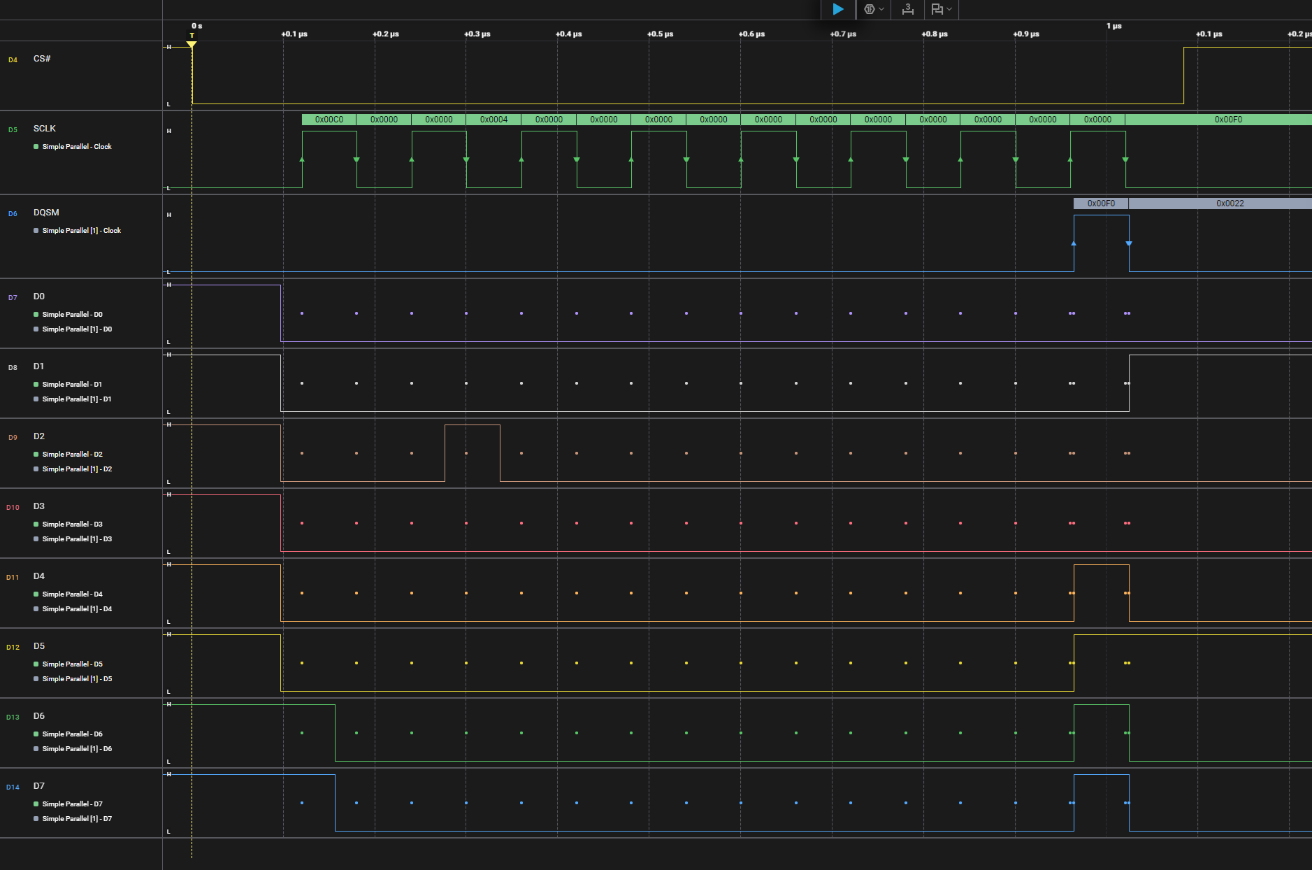
If I enable the PHY mode I'll only get one SCLK cycle which is of course not enough to trigger address, and the necessary dummy cycles until the DQS signal is given.

phy-enabled-cmd-read.png
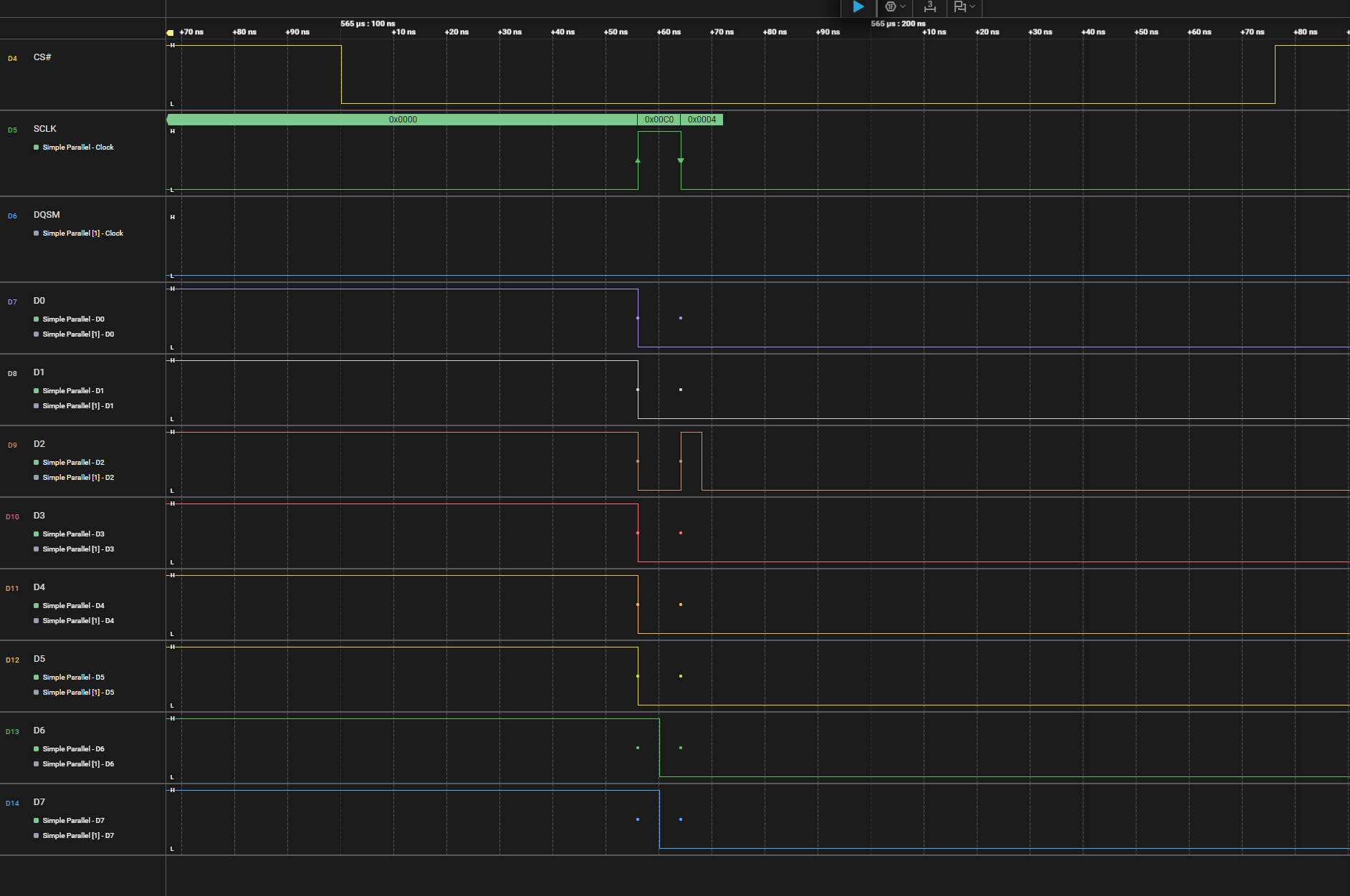
What am I missing to correctly configure the PHY Mode?

The relevant phy configuration (omitting configuration of address and dummy cycles which seems to work with disabled phys):

/* Select the number of delay element to be inserted between
     * phase detect flip-flops.
     */
    CSL_REG32_FINS(&ospi1_flash_cfg->PHY_MASTER_CONTROL_REG,
                   OSPI_FLASH_CFG_PHY_MASTER_CONTROL_REG_PHY_MASTER_PHASE_DETECT_SELECTOR_FLD,
                   2U);

    /* Configure PHY in Master operational mode */
    CSL_REG32_FINS(&ospi1_flash_cfg->PHY_MASTER_CONTROL_REG,
                   OSPI_FLASH_CFG_PHY_MASTER_CONTROL_REG_PHY_MASTER_BYPASS_MODE_FLD,
                   OSPI_FLASH_CFG_PHY_MASTER_CONTROL_REG_PHY_MASTER_MODE);

    /* Set the read delay */
    CSL_REG32_FINS(&ospi1_flash_cfg->RD_DATA_CAPTURE_REG,
                   OSPI_FLASH_CFG_RD_DATA_CAPTURE_REG_DELAY_FLD,
                   5);
    /* Sampled on rising edge of clock */
    CSL_REG32_FINS(&ospi1_flash_cfg->RD_DATA_CAPTURE_REG,
                   OSPI_FLASH_CFG_RD_DATA_CAPTURE_REG_SAMPLE_EDGE_SEL_FLD,
                   CSL_OSPI_FLASH_CFG_RD_DATA_CAPTURE_REG_SAMPLE_EDGE_SEL_FLD_MAX);

    /* Try RX DLL BYPASS ?? */
    // CSL_REG32_FINS(&ospi1_flash_cfg->PHY_CONFIGURATION_REG, OSPI_FLASH_CFG_PHY_CONFIGURATION_REG_PHY_CONFIG_RX_DLL_BYPASS_FLD, 1);

    /* Set TX DLL delay */
    CSL_REG32_FINS(&ospi1_flash_cfg->PHY_CONFIGURATION_REG,
                   OSPI_FLASH_CFG_PHY_CONFIGURATION_REG_PHY_CONFIG_TX_DLL_DELAY_FLD,
                   6);
    /* Set RX DLL delay */
    CSL_REG32_FINS(&ospi1_flash_cfg->PHY_CONFIGURATION_REG,
                   OSPI_FLASH_CFG_PHY_CONFIGURATION_REG_PHY_CONFIG_RX_DLL_DELAY_FLD,
                   6);

    /* phy enable */
    CSL_REG32_FINS(&ospi1_flash_cfg->CONFIG_REG, OSPI_FLASH_CFG_CONFIG_REG_PHY_MODE_ENABLE_FLD, TRUE);

    uint32_t idleFlag = 0;

    /* Wait for Idle */
    while (idleFlag == 0)
    {
        idleFlag = CSL_REG32_FEXT(&ospi1_flash_cfg->CONFIG_REG,
                                  OSPI_FLASH_CFG_CONFIG_REG_IDLE_FLD);
    }

    /* Disable OSPI Controller */
    CSL_REG32_FINS(&ospi1_flash_cfg->CONFIG_REG,
                   OSPI_FLASH_CFG_CONFIG_REG_ENB_SPI_FLD,
                   FALSE);

    /* Clear the delay line resync bit */
    CSL_REG32_FINS(&ospi1_flash_cfg->PHY_CONFIGURATION_REG,
                   OSPI_FLASH_CFG_PHY_CONFIGURATION_REG_PHY_CONFIG_RESYNC_FLD,
                   0U);

    /* Reset DLL in master mode */
    CSL_REG32_FINS(&ospi1_flash_cfg->PHY_CONFIGURATION_REG,
                   OSPI_FLASH_CFG_PHY_CONFIGURATION_REG_PHY_CONFIG_RESET_FLD,
                   0U);

    /* Set Initial delay for the master DLL */
    CSL_REG32_FINS(&ospi1_flash_cfg->PHY_MASTER_CONTROL_REG,
                   OSPI_FLASH_CFG_PHY_MASTER_CONTROL_REG_PHY_MASTER_INITIAL_DELAY_FLD,
                   0x5U);

    /* DLL out of reset */
    CSL_REG32_FINS(&ospi1_flash_cfg->PHY_CONFIGURATION_REG,
                   OSPI_FLASH_CFG_PHY_CONFIGURATION_REG_PHY_CONFIG_RESET_FLD,
                   1U);

    /* Wait DLL lock done */
    while ((CSL_REG32_FEXT(&ospi1_flash_cfg->DLL_OBSERVABLE_LOWER_REG,
                           OSPI_FLASH_CFG_DLL_OBSERVABLE_LOWER_REG_DLL_OBSERVABLE_LOWER_DLL_LOCK_FLD) == 0U))
    {
        (void)idleFlag;
    }

    /* Wait DLL loopback lock done */
    while ((CSL_REG32_FEXT(&ospi1_flash_cfg->DLL_OBSERVABLE_LOWER_REG,
                           OSPI_FLASH_CFG_DLL_OBSERVABLE_LOWER_REG_DLL_OBSERVABLE_LOWER_LOOPBACK_LOCK_FLD) == 0U))
    {
        (void)idleFlag;
    }

    /* Resync the Slave DLLs */
    CSL_REG32_FINS(&ospi1_flash_cfg->PHY_CONFIGURATION_REG,
                   OSPI_FLASH_CFG_PHY_CONFIGURATION_REG_PHY_CONFIG_RESYNC_FLD,
                   1U);

    /* enable SPI */
    CSL_REG32_FINS(&ospi1_flash_cfg->CONFIG_REG,
                   OSPI_FLASH_CFG_CONFIG_REG_ENB_SPI_FLD,
                   1);
  • Hi Jan,

    I have re-assigned the thread to the correct owner, please allow the expert some time to get back.

    Regards,
    Shaunak

  • Hi,

    We have not fully tested PSRAM with Phy integration. This is mentioned in the release notes as well

    MCUSDK-14636 AM261x: Phy Tuning not supported for NAND Flash and PSRAM OSPI, Flash 10.02.00 onwards

    dev.ti.com/.../RELEASE_NOTES_11_01_00_PAGE.html

    My suggestion would be to use non phy mode, until it is tested from our end.

  • As you hopefully see in the code I'm not using the SDK and I am fine to implement the driver for the PSRAM integration myself. I would appreciate getting more information how to use the PHY part of the OSP1 to allow using the DQS to sample the data correctly. 

  • Hi Jan,

    The OSPI 0 IP is the same as OSPI1. If you are looking for a reference on PHY integration, you can refer to the OSPI 0 driver.

    github.com/.../v0

    The untested feature is not related to the code; it's related to the reliable operation of the OSPPHY and signal integrity at different temp ranges

    https://www.ti.com/lit/an/spract2/spract2.pdf

    You can read more about OSPi phy tuning above.

    Let me know if you have further questions.

  • Thanks for your answer.

    I was not aware of this PDF.

    I'm still puzzled what I have to configure in the PHY_MASTER_CONTROL_REG:

    What's the initiator delay?

    What's the intial delay value for the DLL?

    What's the number of increment/decrement indications?

    Furthermore, it seems that the DDR_READ_DELAY_FLD does nothing in the PHY Mode with DQS and DDR enabled. How is it idfferent to the DELAY_FLD in the RD_DATA_CAPTURE_REG?

    Can I influence how many bytes are read in direct access either with PHY_PIPELINE mode enabled or not.

    I'm trying all possible RX_DLL_DELAY_FLD and DELAY_FLD combinations with known data from the PSRAM with PHY Mode active, but I don't seem to get reliable reads above 25mhz. Are the more important tuning parameters which I am missing?
    More information about the register would be greatly appreciated.

  • Hi,
    Currently phy tuning is not enabled for PSRAM, but we are working on enabling it. Sorry  for the delayed response.
    Regards
    Shivank 

  • Hi Jan,

    Thanks for the detailed questions. I'm happy to dive deeper into the OSPI PHY configuration for PSRAM integration with the AM2612. As has been mentioned, dedicated PSRAM PHY tuning isn't fully validated, but we want to provide as much guidance as possible to support your efforts.

    Let's address your questions one by one:

    1. PHY_MASTER_CONTROL_REG - Initiator Delay & Initial DLL Delay

    • Initiator Delay (PHY_MASTER_PHASE_DETECT_SELECTOR_FLD): This field selects the phase detector tap within the PHY. The optimal value is highly dependent on the board layout, trace lengths, and signal integrity. A starting point is 2, as you’ve already tried, but you’ll need to experiment. Higher values increase the delay detection range, potentially improving lock but also introducing instability if set too high. It's crucial to analyze the DQS-to-DQ relationship on an oscilloscope when adjusting this.
    • Initial DLL Delay (PHY_MASTER_INITIAL_DELAY_FLD): This sets the initial coarse delay for the DLL. 0x5 is a reasonable starting point. This value biases the DLL towards a potentially correct delay, speeding up the lock process. Too low or too high can prevent the DLL from converging.

    Important: The DLL lock process is iterative. The PHY detects phase differences and adjusts the delay continuously. These initial values simply provide a starting point for that process.

    2. RD_DATA_CAPTURE_REG vs. PHY Configuration - DDR_READ_DELAY_FLD vs. DELAY_FLD

    You are correct to be puzzled by this! In PHY mode with DQS enabled, the DDR_READ_DELAY_FLD is effectively ignored. The DQS signal provides the timing reference for data sampling, making the static delay adjustment in DDR_READ_DELAY_FLD irrelevant. The DELAY_FLD in RD_DATA_CAPTURE_REG is a legacy setting for non-PHY modes. Focus exclusively on the PHY configuration registers (DLL delay, phase detector selection) when using DQS.

    3. Burst Length Control

    No, there isn't a direct mechanism to modify the burst length within the PHY itself. The burst length is controlled by the OSPI controller configuration (addressing and timing setup). PHY_PIPELINE mode doesn't alter this. You define the burst length using the OSPI registers, and the PHY handles the data transfer in accordance with that defined burst.

    4. DLL Lock Detail

    Unfortunately, the visible DLL lock flags (DLL_OBSERVABLE_LOWER_REG) are fairly coarse. There aren’t readily accessible, more detailed debug registers currently exposed. However, you can indirectly monitor the DLL's behavior:

    • Data Eye Analysis: Use an oscilloscope to examine the data eye opening at the DQ pins. A tight, clear eye indicates good DLL lock. A closed or distorted eye suggests the DLL isn't converging properly.
    • DLL Reset/Resync Cycle: Experiment with the PHY_CONFIG_RESET_FLD and PHY_CONFIG_RESYNC_FLD registers. Repeatedly resetting and resyncing the DLL might help it find a stable lock point, especially if it's getting stuck due to a slight initial imbalance.

    5. DQS Skew

    DQS skew is extremely important. Any significant skew between the DQS and DQ signals will severely impact data sampling.

    • Layout: The most critical factor is careful PCB layout. Keep the DQS and DQ traces as closely matched in length as possible. Minimize vias and bends.
    • Trace Impedance: Ensure consistent impedance control for all traces.
    • Termination: Proper termination is vital to minimize reflections and ringing. Consult the PSRAM datasheet for recommended termination schemes.
    • DQS Calibration (Advanced): While the AM2612 doesn’t have an automated DQS calibration feature, you could potentially implement a software-based calibration routine to fine-tune the DLL delay to compensate for skew. This would involve reading back data with slightly varying DLL settings and analyzing the error rate.

    Further Considerations:

    • Temperature: DLL performance can drift with temperature. Thorough testing across the operating temperature range is essential.
    • Power Supply Noise: Noise on the power supply can affect the PHY's stability. Ensure a clean, stable power supply.
    • PSRAM Datasheet: Carefully review the IS66WV032 datasheet for specific timing requirements and recommendations.

    We are happy to continue this conversation and provide further assistance. Please feel free to share your test results and any specific waveforms you capture.

    Best Regards,

    Zackary Fleenor