ADS1278EVM-PDK: Interfacing ADS1278EVM-PDK with ARM microcontroller

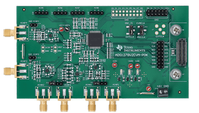
Part Number: ADS1278EVM-PDK
Other Parts Discussed in Thread: ADS1278, ADS127L18

Hello,

I have been looking to interface the ADS1278EVM-PDK from an arm microcontroller using a SPI interface, via the external controller options outlined in the datasheet. I am having some difficulty transferring data (the clock/ drdy pins seem to be functioning, but there seems to be issues reading the data. I have noticed several of the chips available have example drivers/ device tree overlays, are any of these available for this chip/device?

Best Regards,
Joseph Sutlive 

  • Hello Joseph,

    No, unfortunately we do not have any example code for the ADS1278.  If you can capture a SPI frame using an oscilloscope or logic analyzer and share a screen shot, I will look it over for possible timing issues.  Please capture the /DRDY, SCLK, DOUT1 signals.

    Also, we recently updated the EVM, so I am not sure which one you are using.  Please confirm you have the V2 version, per the below image.

    We have a newer generation device that you may also want to consider, the ADS127L18.  We have example code for this ADC.

    https://www.ti.com/tool/download/ADS127L18-FPGA-EXAMPLE-CODE

    https://www.ti.com/tool/download/ADS127L18-MSPM0-EXAMPLE-CODE

    Regards,
    Keith Nicholas
    Precision ADC Applications  

  • Hi Keith,

    Thanks for your answer, I'll definitely look into the new generation device.
    In the meantime, I have attached the timing of a SPI frame. The SPI clock is set to 1 MHz on the controller side. We are using the device on low-speed mode, SPI discrete format, with the CLKDIV pins open. We are using the V2 EVM.

    Thanks again for your help!

    Best,
    Joseph Sutlive

  • Hello Joseph,

    It appears you are using a Saleae logic analyzer.  Please send the *.sal logic capture file.  This will be easier to look at timing than the screenshot.  Also, your SCLK duty cycle seems to vary quite a bit.  If possible, increase the sample rate on your logic analyzer.  Disabling all non-used channels can help with this.

    Also, I'm not sure how you have made the connections to your board.  Please refer to below on an example setup and make sure you have configured all signals properly.

    Directions to connect ADS1278EVM to external MCU

    In order to use the ADS1278EVM board with an external controller, you need to remove the PHI board, otherwise, the digital lines will be driven by the PHI board preventing correct operation with an external MCU.

    1.  Provide +6V on J10 from an external bench supply.

    2.  Move jumper JP1 to the 27MHz position, this enables the on-board 27MHz oscillator.

    3.  Move jumper JP2 to the EVMCLK position, this selects the on-board 27MHz oscillator.

    4.  You may need to install jumpers on J4, depending on the mode of operation that you want to use.  For example, configure ADC for high-speed, SPI, TDM, Dynamic, then you will need to install jumpers on MODE0, MODE1, FORMAT0, FORMAT1, and FORMAT2.  CLKDIV should remain open (high).

    For the SPI connections on J6:

    1.  MISO -> DOUT1

    2.  SCLK -> SCLK

    3.  Connect DIN to GND, do not leave floating.

    4.  Connect /SYNC to an IO pin on your MCU (needed for robust power-up reset), or tie to IOVDD for test purposes.

    5.  Connect /DRDY to an IO pin your MCU.  This is an output from the ADC, indicating when data are ready to be read.  The code should monitor this pin (polling or interrupt) and only transfer data after a falling edge (Figure 77).

    Regards,
    Keith

  • Hi Keith, 

     The MCU I'm currently using is a rasbperry pi 4. I have tied DRDY to a gpio, SCLK to SCLK, DOUT1 to MISO, and SYNC to 3.3V. I've also tied DIN to GND. The device is set in low-speed mode, SPI Discrete format, with fMOD = fCLK/40.

    The logic analyzer is being sampled at 100 MS/s. It says I can't attach the .SAL files here? Is there a possible other solution for this?

    Thanks,
    Joseph Sutlive

  • Hello Joseph,

    Using discrete mode will use all 8 DOUT lines, 1 for each of the ADC channels.  Unless you have 8 SPI ports on your processor, I do not think this mode will work for you.  I suggest using TDM mode (fixed or dynamic) which will interleave all 8 channels over the DOUT1 pin.  However, for debug purposes, you can keep it in discrete mode and just focus on correctly reading data from a single ADC channel.

    I have been able to attach *.sal files in the past, but it is possible this has been disabled.  I do not think drag and drop will work; use the Insert->Image/Video/File option if you did not already do this.  It may be worth trying a second time just in case.  Also, you could change the extension to *.txt; that may allow the file to be attached and then I can change it back to *.sal to view with the Logic software.

    If all else fails, try attaching another image.  In this case, capture the falling edge of /DRDY in the image, and then show the 24 SCLKs as well as the DOUT1 line.  You must read the data before the next conversion result is ready.  With 27MHz clock and fmod=fclk/40, your data rate will be 10.5ksps.  You will need to read the 24b result in less than the 94us conversion rate period.  If you wait too long after the /DRDY falling edge before clocking the data out, then you will get corrupted data.

    Also, this could be an input configuration issue.  What input voltage are you trying to measure in this test case?  If you could provide an a sketch on how you have the inputs connected that may be helpful.

    I will be out of the office next Monday; I will respond next Tuesday with any follow-up questions.

    Regards,
    Keith