This thread has been locked.

If you have a related question, please click the "Ask a related question" button in the top right corner. The newly created question will be automatically linked to this question.

TXS0104V: Interfacing a 3.3 V I2C Keypad with STM32U5G9J-DK1 via TXS0104VDR for 3.3 V-to-1.8 V level shifting

Part Number: TXS0104V
Other Parts Discussed in Thread: LSF0108

Hello all,

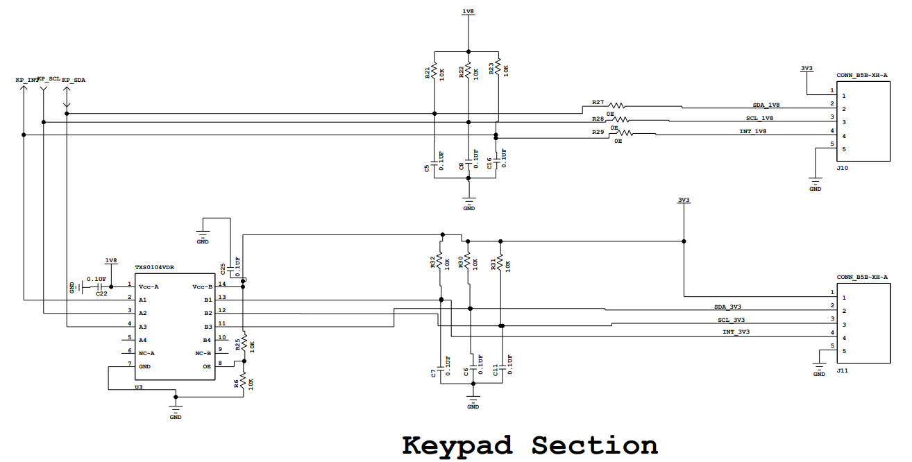
I want to connect a 3.3 V I2C based keypad with STM32U5G9J-DK1 via a carrier board on which the STM32 board sits via expansion connectors CN9 and CN10 present on it. I am using pins PG13, PG14, and PG9 for my I2C SDA, I2C SCL, and INTERRUPT, which are available as Pin No. 4, 2, and 8 respectively on CN10. The signals pass through TXS0104VDR on the carrier board for conversion between 1.8 V signals at the STM32 end and 3.3 V signals at the keypad end.

These lines are also connected with external pull up resistors as indicated in images attached. All the capacitors between the signal lines and GND have been unmounted. Also, 0 Ohm resistors (R27, R28, and R29 have been unmounted).

During operation, STM32 can't detect any I2C device connected whereas the keypad seems to work perfectly when used in a different setup. Upon further investigation, it appears that all the three pins have become unresponsive, even when the board is used standalone, disengaged from the carrier board. Setting internal pull-ups via STMCube doesn't show up when these pins are probed for the same. Similarly, interrupts aren't detected via STM32 MCU even when interrupts are applied on the pins externally.

I suppose some design flaw is to be blamed for this malfunctioning and I hope you can help me diagnose it.Screenshot 2026-03-23 113804.pngScreenshot 2026-03-23 113841.png

  • Hi Gaurav,

    Are there any waveforms between the I/Os that was captured to show the ch. of the signals? Note the external pullups can be removed from the I/Os, as the device has internal 10kohm pullups already. Any external pullups used will result shifted VOL levels: www.ti.com/.../scea054a.pdf

    Regards,

    Jack

  • Since pins on the MCU (master side) have become unresponsive, no waveforms are generated for SCL/SDA lines. However, I can still generate waveforms for INTERRUPT by pressing keys on my keypad. It is an ACTIVE LOW INTERRUPT and waveform shows 3.3 V to 0 V and then back to 3.3 V transition upon key press. On the other side of the level shifter, I get a similar waveform showing 1.8 V to 0 V and back to 1.8 V transition which was probed on pin PG9. However, the INTERRUPT isn't detetcted by the MCU, indicating that the pin might be unresponsive to MCU.

  • Hi Gaurav,

    I would suggest reaching out to MCU vendor here to debug. From the description provided, it seems that the level shifter is working as expected-please let me know if I am misunderstanding: 

    waveform shows 3.3 V to 0 V and then back to 3.3 V transition upon key press. On the other side of the level shifter, I get a similar waveform showing 1.8 V to 0 V and back to 1.8 V transition

    Regards,

    Jack

  • While, the level shifter is working as expected, I fear the design around the level shifter comprising of the external pull-ups has affected the MCU due to which this erratic behaviour shows up.

  • Hi Gaurav,

    For alternative level shifters in this application, there is also the LSF0108 that is an open-drain supported level shifter that requires external pullups at the I/Os. This device can be used if you believe there are some concerns revolving around the pullups situation. 

    Regards,

    Jack 

  • Thanks for the recommendation.

    Regards,

    gaurav