


Part Number: MSPM0G3519
Other Parts Discussed in Thread: MSPM0G3218
Hi Ti Team,
I have one question regarding VREF of MSPM0G3218 chip
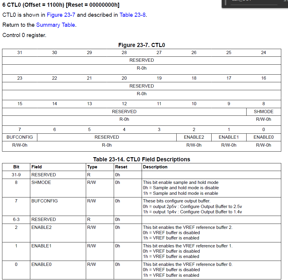 At the moment, I see that we have 3 enable channel for CTL0 of VREF. I configure BUFCONFIG as 0 (output 2p5v) . Then I set ENABLE2 to 1 , I understand that now VREF2 is enabled (I can measure the voltage here using ADC1). If then I set ENABLE1 to 1, I understand that now VREF1 is enabled and connected to internal 2.5V as well.
My question is:
1) Is it possible that I configure VREF1 using external voltage reference, while VREF2 using internal voltage (2p5V) ?
2) What is the purpose of VREF0 in here ? What is the difference betwen VREF0, VREF1 and VREF2 ? I cannot see the difference in the datasheet
