


Part Number: AM2612
Hi Team,
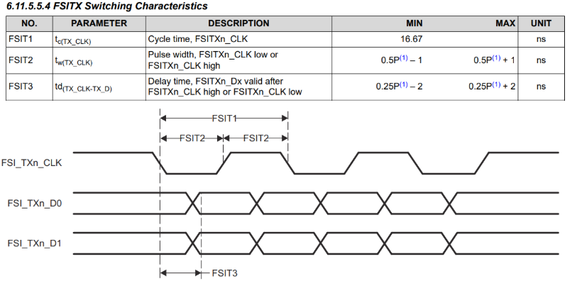
In my design I connect the am2612 MCU to a FPGA via the FSI interface. I am doing the timing analysis to see how much setup time and hold time I can have. But the timing characteristics of FSI TX is not clear to me.
- Is FSIT2 the actual measured value in the pad?
- Is FSIT3 is measured related to the ideal internal FSI TX clock inside the MCU or it is actually related to the actual FSITX_CLK output waveform, whose duty‑cycle distortion is already captured by FSIT2?
Thank you in advance for your help,
Y.Zhao
