AM2634-Q1: ZCZ_F package with internal Flash, Flash is not accesible

Part Number: AM2634-Q1
Other Parts Discussed in Thread: AM263P4, UNIFLASH

AM263P4 has the correct V1.2v and V3.3 supplied.

R2 PORz is pulled up

C3 WARMRSTn pulled high

J3 OSPI0_ZCZ_F_RESET_OUT0 pulled low

L1 OSPI0_ZCZ_F_WP pulled high

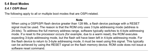
All of the following steps have been test on an AM263P4-SIP control card and our custom hardware

  1. Use Uniflash in JTAG mode to program the internal flash, failed on custom hardware
  2. Use Uniflash in serial mode to program internal flash, failed custom hardware
  3. Using code composer loaded simple app in RAM to custom hardware, worked as expected.
  4. Modifed SDK OSPI Flash Diag example to provide more details about the Flash.
  5. Ran Diag tool on Control card, reports expected Flash information 
  6. Ran Diag tool on custom hardware, Status register read from flash is 0xff.

At this point we have exhausted the list of things that we can verify or test.  The fact that the AM263P4 is able to run code is ram gives us some confidence that the part is correctly conneced.

What are we missing or what should we try to get the flash working on our custom hardware?

  • Hi Jeffrey,

    Apologies for the delay in response!

    J3 OSPI0_ZCZ_F_RESET_OUT0 pulled low

    J3 should not be pulled low. (This the the reset line to the SIP-Flash.)

    In AM263P-SIP device the J3 pin (RESET_OUT0 ) is an output from the AM263P4 that drives the flash reset line. It is an Active LOW signal - means pulling it low = puts flash in reset (disabled, unresponsive). Pulling it LOW externally forces the flash into permanent reset state, which explains the 0xFF status register read (no response from flash).

    • The ZCZ_F packages offers an internally connected on-die OSPI flash module (ISSI IS25LX064-JWLA3 OSPI Flash device). Due to the internal connections, the ZCZ_F package comes with additional pin connection requirements. Please reference Pin Connectivity Requirements in datasheet for pin connectivity requirements and ball names.
    • The OSPI_D2 signal of Flash die (pin L1-OSPI0_ZCZ_F_WP) doubles as the active low Write Protect input for the internally connected flash device. Therefore, pin L1-OSPI0_ZCZ_F_WP must be connected to the relevant source (VDDS33) through a separate 4.7kΩ external pull resistor. This resistor must be placed as close to the device as possible.
    • The OSPI_RESET_OUT0 signal of Flash die (pin J3-OSPI0_ZCZ_F_RESET_OUT0) must be connected to an open-drain equivalent of WARMRSTn in order to reset the on-die OSPI flash module. The open-drain requirement is to prevent a bus contention between the external WARMRSTn connection via pin J3-OSPI0_ZCZ_F_RESET_OUT0 and the package internal connection between the AM263P and the OSPI flash device.


    In Summary, there are 2 sources toi reset the flash

    1.  Warmreset Pin (Covering the internal and external warmreset sources) - this is done inorder to cover reruiremnt not in section 5.4.1 OSPI BOOT
    2. OSPI0_ZCZ_F_RESET_OUT0 - Reset signal to flash from the OSIP0_Controller (triggered using MMR configurations ) connected internally from AM263p die to Flash die inside SIP package


    Refer to Section 8.1.3 OSPI Connections for Flash-in-Package (ZCZ_F) in AM263P Datasheet for more details.

    Please let me know if you have any questions or if this resolves the issue.

    Thanks & Regards,
    Rijohn

  • Rijohn,

    I see that I made a mistake in the original problem statement.  We compared the connection to J3 on our hardware vs the control card.  The circuit we use is the same as what is shown in the control card schematic page 14 OSPI Flash Reset.  The output of Q21 is high on the control card.  The equivalent transistor for our hardware is the same also high.

    I apologize for the confusion.

    Jeff

  • Rijohn,

    Your information was correct.  We were indeed driving the OSPI reset low.  The source for the error was using the schematic for the PROCA version of the control card.  This version of the schematic show an N-channel mosfet.  We discovered today that this was corrected in the PROCB version of the control card has this corrected.

    Thank you for the help.

    Jeff

  • Hi Jeff,

    Thank you for the reply. 

    Glad that you were able to figure out the change in buffer implementation from Rev A to REVB revision of the board.
    FYI, These changes are mentioned the revision history section (at the start) of the schematic document.

    Thanks & Regards,
    Rijohn

  • Rijohn,

    We did see the PROCB schematic after your initial response.  The reason we were confused is that we have a PROCA SIP board.  It was reworked before it was shipped to correct Q21.  The source of confusion is that the PROCA board worked as expected.

    Jeff

  • Hi Jeffy,

    Sorry for the delay!!

    The source of confusion is that the PROCA board worked as expected.

    I get what you are saying, this was was mistake from our side. We initially made a mistake in keeping a nMOS instead of pMOS in the OSPI reset logic to J3 pin. PROCA version has Q21 (BSS138LT1G) which is an n-channel MOSFET in schematic. Causing the inversion operation of what is expected.

    Input (PORz) MOSFET State Output (OSPI_RSTn_R)
    LOW  OFF HIGH (3.3V) via R3878 pull-up
    HIGH  ON LOW (0V) pulled to DGND


    This error was caught during initial board testing itself and hence component was changed to pMOS, rotated and flipped(in Z-axis) to attain the needed functionality of the buffer as in the image below.

    Sincere apologies for the confusion caused.

    Q21-PMOS Flip


    Thanks & Regards,
    Rijohn