AM263P4: ADC2 reference error during initialization.

Part Number: AM263P4
Other Parts Discussed in Thread: SYSCONFIG

Hi Experts,

My customer is seeing ADC2 reference error on R5_3 during OSPI boot, where all 4 cores are used and all of them uses at least one ADC instance. There is no issue debuging R5_3 alone in dev boot.

Below is the info we saw after connecting to the R5_3 after booting the deivce in OSPI boot.

173D15D0-0A4E-47EB-9071-82A907713C99.png

As you can see, the CPu is blocked in the asset function, I believe it sholud be line 57 assert instad of line 61, correct?

If so, the issue is related to ADC reference.

This is ADC2 instance which is connected to ADC_VREFHI_G0


image.png

We have comfirmed the volatge on G1 is 1.8V.

And also tried to disconnect the pin from the 1.8V LDO reference, both have the same issue.

And we also tried disabling internel buffer 0 in the syscfg
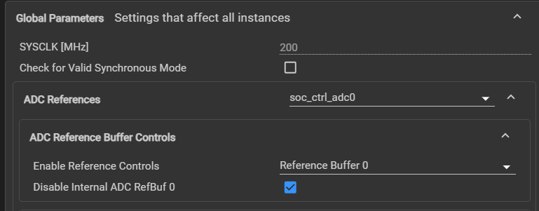
image.png

Although ADC2 is not connected to buffer0 from the diagram, we are still seeing in the syscfg, when you hover on the disalbe option, it says that "dsiable buffer0 is for ADC0,1,2". We don't know whether it's a error of the diagram or syscfg. Anyway, we tried disabled it, but the issue remains.

May I know what might be the issue here?

SDK version 11.0.0.19

Sysconfig version 1.25

Regards,

Hang


  • Hi Hang,

    Your read is correct. The call stack shows R5_3 suspended in _DebugP_assert() (DebugP_log.c:105) called from Drivers_open(). Line 61 is SOC_enableAdcDacLoopback(FALSE), which contains no assert; the only assert in that region is line 57:

    SOC_enableAdcInternalReference(2, FALSE);   // line 48
    SOC_enableAdcReferenceMonitor(2, TRUE);     // line 51
    ClockP_usleep(1);                           // line 54
    DebugP_assert(SOC_getAdcReferenceStatus(2) == true);  // line 57  <-- fails
    

    SOC_getAdcReferenceStatus() returns TRUE only when the reference is OK, FALSE when not OK 1. So the ADC2 reference-good monitor is reporting not-ready/invalid 1 µs after the monitor was enabled.

    Most likely cause: 1 µs settling delay vs. documented ADC power-up time

    The datasheet specifies an ADC power-up time of up to 500 µs, while the generated code waits only ClockP_usleep(1) before asserting 2. This is the strongest explanation for a failure that is boot-order/timing dependent — in a single-core dev-boot debug session the reference path has typically already been powered and settled by the time you step through Drivers_open(), whereas in cold OSPI boot R5_3 reaches this check much earlier relative to reference power-up.

    TI also documents a related transient risk: the TOP_CTRL_MASK_ANA_ISO register exists specifically to mask a momentary "Ana ISO" SOC-reset glitch that can occur when ADC reference buffers are enabled 3 — i.e., the enable sequence has a known non-instantaneous/glitch-prone window.

    A second contributing factor specific to your 4-core setup: the ADC1/ADC2 reference monitor is not per-instance. TOP_CTRL_ADC_REF_COMP_CTRL has a single ADC_REF_COMP_CTRL_ADC12_REFOK_EN field that "monitors adc1 & adc2 reference" 4, and TOP_CTRL_ADC_REF_GOOD_STATUS reports combined ADC12_REF_UV_GOOD/OV_GOOD bits for the pair 5. Since Drivers_open() runs once per core and each core generates its own ADC reference/monitor writes 6, two cores configuring ADC1 and ADC2 touch the same shared global MMR field. Whether that ordering actually clears/re-arms the monitor under R5_3 is not documented — flagged as a gap below.

    Note: ADC2 is on reference group G1, not G0

    Your block diagram shows ADC1 and ADC2 both routed in parallel to ADC_VREFHI_G1 and ADC_VREFLO_G1. G0 and G1 are physically distinct nets on distinct balls — ADC_VREFHI_G1/ADC_VREFLO_G1 at V10/V11 versus ADC_VREFHI_G0/ADC_VREFLO_G0 at V14/V13 7. The decoupling table further groups ADC_VREFHI_G[1:0] under one spec with G[2] and G[3] separate, reinforcing that these are not interchangeable labels 8.

    So your statement "ADC2 is connected to ADC_VREFHI_G0" is the error — G1 is the net that matters for ADC2, which is consistent with you measuring 1.8V on G1. Confirm that 1.8V is within the required VREFHI range of 1.71–1.89 V 2 at the ball, under load, during the boot window.


    Buffer 0 vs. the diagram — why disabling it changed nothing

    The AM263Px reference connectivity diagram (Figure 2-6) shows three internal buffers — REFBUF0, REFBUF1, REFBUF2 — routed across ADC0–ADC4 and groups G0/G1/G2/G3, which is a different topology from the simpler non-Px AM263x figure 9.

    Two consequences:

    • REFBUF0 and REFBUF1 are controlled by separate registers (TOP_CTRL_ADC_REFBUF0_CTRL, TOP_CTRL_ADC_REFBUF1_CTRL), each with its own 3-bit enable field 10. So "Reference Buffer 0" in SysConfig may simply not be the buffer gating the ADC1/ADC2 (G1) path being monitored — which would explain why checking "Disable Internal ADC RefBuf 0" had no effect.
    • Disabling the internal buffer does not bypass the monitor. The generated code still calls SOC_enableAdcReferenceMonitor(2, TRUE) — which only writes the Control MMR enable 1 — and then asserts on the status 1 µs later regardless. Hence "issue remains."

    Recommended actions:

    In priority order:

    1. Increase the settling delay first. Temporarily raise the delay before the line-57 check from 1 µs to ≥500 µs (or poll SOC_getAdcReferenceStatus(2) in a timed loop instead of asserting immediately). If the assert clears, the root cause is the insufficient generated delay versus the 500 µs power-up spec 2. Note this is a generated file — apply via a local patch for the experiment, then raise it with TI for a SysConfig-side fix.
    2. Read the raw status directly. Dump TOP_CTRL_ADC_REF_GOOD_STATUS to see whether ADC12_REF_UV_GOOD or ADC12_REF_OV_GOOD is the failing bit 5 — undervoltage vs. overvoltage points at very different board-level causes.
    3. Deconflict the shared ADC1/ADC2 monitor across cores. Because ADC12_REFOK_EN is one shared field for both instances 4, have only one core own the global ADC reference/monitor configuration (disable the reference-control generation in the other cores' SysConfig) and confirm that core completes before R5_3 reaches its check.
    4. Fix the SysConfig reference-group selection. Since ADC2 is on G1, verify the ADC reference settings target the G1/correct buffer path rather than Buffer 0 — and re-validate external 1.8V and decoupling on the ADC_VREFHI_G[1:0] net per the hardware design guide 8.
    5. Check Ana ISO masking in your boot/SBL flow, given the documented reset-glitch condition tied to reference-buffer enable 3.


    1. MCU+ SDK AM263Px 11.00.00.19 — SOC Module API Guide
    2. AM263P4 Datasheet — ADC Electrical Characteristics (p.80)
    3. AM263Px Technical Reference Manual — TOP_CTRL_MASK_ANA_ISO (p.53)
    4. AM263Px TRM — TOP_CTRL_ADC_REF_COMP_CTRL (p.42)
    5. AM263Px TRM — TOP_CTRL_ADC_REF_GOOD_STATUS (p.43)
    6. AM26x Academy — SysConfig / Drivers_open generation
    7. AM263P4 Datasheet — Signal/Pin Table (p.51)
    8. AM263Px Hardware Design Guide — Decoupling Requirements (p.18)
    9. AM263Px Hardware Design Guide — ADC Reference Connectivity, Figure 2-6 (p.19)
    10. AM263Px TRM — TOP_CTRL_ADC_REFBUF0/1_CTRL (p.40)
    11. MCU+ SDK AM263Px 26.00.00.06 — SOC Module API Guide
    12. E2E: AM263P4 OSPI Boot — SBL Failed Error

    Best Regards,

    Zackary Fleenor

  • Hi Fleenor,

    The concerned external reference pin is G1, the G0 above is a typo. We had ensured that the G1 has 1.8V.

    For recommended action:

    1. Increase the settling delay first. This is a sysconfig code. Not alterable.

    4. Already checked as said above.

    I'll see if rest of the measures can work.

    Regards,

    Hang