This thread has been locked.

If you have a related question, please click the "Ask a related question" button in the top right corner. The newly created question will be automatically linked to this question.

DMA from Timer Capture interrupt including GPIO

Other Parts Discussed in Thread: EK-LM3S9D92

Hi all, first post to the forum, but I have already learned a lot from reading the excellent material available!

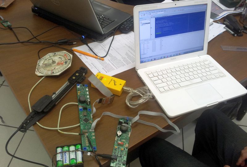
My aim on this thread is to measure duty cycle and width of an external PWM signal. I am developing on the LaunchPad with the now called TM4C1233H6. Workspace is IAR.

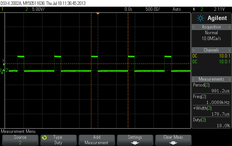
My PWM signal inputs to Timer2A via PF4 pin. Its typical width is 990us. The duty cycle can be as small as a 1us ON time (image below displays the signal at 18% duty cycle, with 178us ON time).

Timer2A is configured as half width (16bit), capture mode counting up (TIMER_CFG_SPLIT_PAIR|TIMER_CFG_A_CAP_TIME_UP), and the interrupt is enabled for BOTH_EDGES.

Measuring strategy is to read the TAR whenever it triggers a capture, and at the same time read the GPIO of PF4 to determine if the board was going up or down. The difference between two "going up" borders is the width, and the difference between "going down" minus "going up" is the proportional ON time. The reason why the full width is read, and not only assumed constant, is because the sensor that generates the signal is a little unstable, and can vary the full width by about 1%.

All working good so far, but on the edges of the sensor range, the 1us interval is too short to treat the interrupt routine and properly read the timers before the opposite border capture would happen.

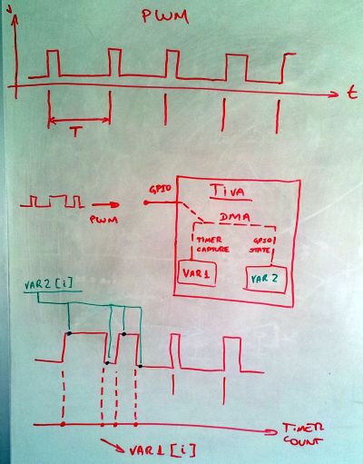
So the idea is to DMA two values to a buffer area in memory: the Timer2A TAR register AND the GPIO F register at the moment of the border interrupt, so that the processor can deal with calculations later when there is free time. Because of the other processing tasks, I would like a buffer with some 16 readings of those two registers. The DMA transfer should circle back to the first address, after storing into location #16.

I am still on the very first steps of DMA (I should say crawling), but I can't quite understand how to transfer TWO peripheral values via DMA triggered by one same interrupt (the event capture of the GP Timer). I would appreciate suggestions for this solution (and actually even for the more basic task of transferring only the Timer2 TAR register via DMA). 

Thanks in advance!

  • Hi Bruno,

    Welcome to the forum!  We do have an example that would be a helpful starting place for you.  If you download the final version of StellarisWare  for the EK-LM3S9D92 from here: http://www.ti.com/tool/sw-ek-lm3s9b92, you can find the udma_timer_ccp example that should help get you started.

    The uDMA is designed to work with different modules independently, so your best bet is to set up the uDMA triggers for both the timer and the GPIO.  Obviously, they can't both operate at exactly the same time, but the difference in the number of clocks should be small.

    Regards,

    Sue

  • Hi Sue and TI,

    After the question above, we got our product running on the market for a while, simply using DMA on the Timer Capture and "quickly" looking at the GPIO status right after the last DMA interrupt.

    However, we still left some glitches with that solution, particularly when the PWM duty is too small, with the last ON period of the pin being close to just 1ms. And now adding other functions to our code that hinder a fast interrupt response, this is becoming a problem.

    Now we tried to configure two DMA channels at "the same time" (there are 4 values transfered in one shot). One should transfer the Timer Capture values to a vector, and the other should transfer the GPIO values. I am aware that they can not be exactly at the same time, but a few cycles apart should not be a problem.

    But the results just don't seem correct. What we tried is to tie on DMA channel to Capture up and down, the other on GPIO raise/fall. But the GPIO pin values of that vector are all zeroes, when the expected was alternating 1's and 0's.

    As a debug test, we configured the second DMA source address as the Timer Counter instead of the GPIO address (in which case we would expect both vectors to show very close numbers). Vector #2, initiated by GPIO rise/fall interrupt, shows one or two numbers that coincide with vector #1, and the others are non-related.

    Question: can we really configure two DMA channels driven by THE SAME PHYSICAL GPIO PIN, one as a Timer Capture and one as IO level change?

    And, if so, could anyone provide a configuration sample for capturing the GPIO level via DMA four times, driven by raise/fall borders, working on that same pin which is set as a timer capture?

    Thanks a lot!

  • Hello Bruno,

    Yes it is possible to configure the same GPIO as the source of DMA request since the input function will still work for alternate function selection.

    Regards

    Amit

  • Hi Amit,

    Thanks! Well, something is not right. I guess it is time to paste a more detailed code so that you guys can take a look...

    The code is below. Please look at the print screen. The "something weird" result is that MOST of the times the value of enc_estado[0] is exactly the same as enc_pulsos[0], which is what I expect. But a few random times, enc_estado[0] records what seems to be the previous Timer Capture value, meaning the Timer DMA did not trigger at the same time as the IO DMA.

    Let me know if I can explain any further or test anything else. Otherwise, a suggestion as how to achieve this goal is most welcome!

    //==============================================================================
    //
    // Macros
    //
    //==============================================================================
    
    
    // Macros to control/detect start and conclusion of a data acquisition cycle
    #define encStatus_startDmaCycle()      (enc_status |= ENC_RUNNING_DMA_CYCLE)
    #define encStatus_isRunningDmaCycle()  (enc_status & ENC_RUNNING_DMA_CYCLE)
    #define encStatus_finishDmaCycle()     (enc_status &= ~ENC_RUNNING_DMA_CYCLE)


    //==============================================================================
    //
    // Global Variables
    //
    //==============================================================================
    
    // uDMA configuration table
    #pragma data_alignment=1024
    static uint8_t   enc_DMAControlTable[1024];
    
    // General status (used to indicate end of data acquisition)
    static uint32_t  enc_status;
    
    // Data acquired via DMA
    static int32_t   enc_pulsos[4]; // from Timer DMA channel
    static int32_t   enc_estado[4]; // from GPIO  DMA channel


    //==============================================================================
    //
    // Functions
    //
    //==============================================================================
    
    
    //----------
    // ISR for GPIO, used with uDMA
    //----------
    void GPIOFIntHandler()
    {
     GPIOIntDisable(GPIO_PORTF_BASE, GPIO_PIN_2);
     GPIOIntDisable(GPIO_PORTF_BASE, GPIO_PIN_3);
     GPIOIntDisable(GPIO_PORTF_BASE, GPIO_PIN_4);
     GPIOIntDisable(GPIO_PORTF_BASE, GPIO_PIN_5);
     
     GPIOIntClear(GPIO_PORTF_BASE, GPIO_PIN_2);
     GPIOIntClear(GPIO_PORTF_BASE, GPIO_PIN_3);
     GPIOIntClear(GPIO_PORTF_BASE, GPIO_PIN_4);
     GPIOIntClear(GPIO_PORTF_BASE, GPIO_PIN_5);
    }
    
    
    //----------
    // ISR for Timer 2A DMA, used with uDMA
    //----------
    void Timer2AIntHandler()
    {
     // Turns timer off
     MAP_TimerDisable(TIMER2_BASE, TIMER_A);
     MAP_TimerIntClear(TIMER2_BASE, TIMER_CAPA_EVENT);
     HWREG(TIMER2_BASE + 0x050) = 0;  // Clears timer counting value
    
     // Indicates end of data acquisition
     encStatus_finishDmaCycle();
    }
    
    
    //----------
    // Initializes hardware
    //----------
    void init_hw()
    {
     //----------
     // Initial settings
     //----------
    
     // PF4 - T2CCP0 - Timer 2A
     MAP_SysCtlPeripheralEnable(SYSCTL_PERIPH_GPIOF);
     MAP_GPIOPinConfigure(GPIO_PF4_T2CCP0);
     MAP_GPIOPinTypeTimer(GPIO_PORTF_BASE, GPIO_PIN_4);
     
     // Enables a GPIO pin as a trigger to start a DMA transaction (this works this way?)
     ROM_GPIODMATriggerEnable(GPIO_PORTF_BASE, GPIO_PIN_4);
    
     // Configure interrupt parameters for GPIO, but doe not enable interrupt handling
     ROM_GPIOIntTypeSet(GPIO_PORTF_BASE, GPIO_PIN_4, GPIO_RISING_EDGE);
     GPIOIntDisable(GPIO_PORTF_BASE, GPIO_PIN_4);
     ROM_IntEnable(INT_GPIOF);
     ROM_IntMasterEnable();
    
     //----------
     // Timer 2A settings
     //----------
     
     // Turn timer 2 on
     MAP_SysCtlPeripheralEnable(SYSCTL_PERIPH_TIMER2);
     MAP_SysCtlDelay(10);
     
     // Operation modo "Input Edge-Time Mode"
     MAP_TimerConfigure(
       TIMER2_BASE,
       (
         TIMER_CFG_SPLIT_PAIR    |
         TIMER_CFG_A_CAP_TIME_UP |
         TIMER_CFG_B_CAP_TIME_UP  
       )
     );
     
     // Configures capture mode
     MAP_TimerControlEvent(TIMER2_BASE, TIMER_A, TIMER_EVENT_BOTH_EDGES);
     
     // Enables interrupt
     MAP_IntEnable(INT_TIMER2A);
     
     
     //----------
     // uDMA settings
     //----------
     
     MAP_SysCtlPeripheralEnable(SYSCTL_PERIPH_UDMA);
     MAP_uDMAEnable();
     MAP_uDMAControlBaseSet(enc_DMAControlTable);
     MAP_uDMAChannelSelectSecondary(UDMA_DEF_USBEP3RX_SEC_TMR2A);
     MAP_uDMAChannelControlSet(
       (
         UDMA_SEC_CHANNEL_TMR2A_4 |
         UDMA_PRI_SELECT           
       ),
       (
         UDMA_SIZE_32      |
         UDMA_SRC_INC_NONE |
         UDMA_DST_INC_32   |
         UDMA_ARB_1                
       )
     );
     MAP_uDMAChannelControlSet(
       (
         UDMA_CH15_GPIOF   |
         UDMA_PRI_SELECT    
       ),                  
       (                   
         UDMA_SIZE_32      |
         UDMA_SRC_INC_NONE |
         UDMA_DST_INC_32   |
         UDMA_ARB_1         
       )
     );
     ROM_uDMAChannelAssign(UDMA_CH15_GPIOF);
    }
    
    
    //----------
    // Test function, called in main(): starts a data acquisition and awaits it be concluded
    //----------
    void read_pwm()
    {
     // Enables DMA with Timer 2A
     MAP_uDMAChannelTransferSet(
       (
         UDMA_SEC_CHANNEL_TMR2A_4 |
         UDMA_PRI_SELECT           
       ),
       UDMA_MODE_BASIC,               
       (void *)(TIMER2_BASE + 0x048), 
       enc_pulsos,                    
       4                              
     );
     
     // Enables DMA with GPIO
     MAP_uDMAChannelTransferSet(
       (
         UDMA_CH15_GPIOF |            
         UDMA_PRI_SELECT              
       ),
       UDMA_MODE_BASIC,               
       (void *)(TIMER2_BASE + 0x048),  // Reading timer counting value as a debug strategy:
                                       // we expect the GPIO DMA request occurs almost at
                                       // the same time the TIMER DMA request (so, we expect
                                       // very close values for Timer DMA and GPIO DMA)
       enc_estado,                    
       1                              
     );
    
     // Starts a data acquisition cycle
     MAP_uDMAChannelEnable(UDMA_SEC_CHANNEL_TMR2A_4);
     MAP_uDMAChannelEnable(UDMA_CH15_GPIOF);
     encStatus_startDmaCycle();
     MAP_TimerEnable(TIMER2_BASE, TIMER_A);
     GPIOIntEnable(GPIO_PORTF_BASE, GPIO_PIN_4);
     
     // Expects end of data acquisition
     while( encStatus_isRunningDmaCycle() ) {}
    }

  • Hello Bruno,

    Thanks for the code. Will be able to run it on the LaunchPad next week only. However one thing you may want to try is to zero-init the arrays and reset the peripherals before using them using SysCtlPeripheralEnable API call.

    Regards

    Amit

  • Hi Amit,

    Were you able to run the posted code? The other battle that we were having with timers got properly solved, and I posted our solution on the proper thread. This one is still pending, and your help will be welcome!

    Bruno

  • Hello Bruno,

    Not yet. But surely by Monday I should be able to have a working code (CCS is what I have, but it is more of the actual code than it is the IDE).

    Regards

    Amit

  • Hello Bruno,

    Since I did not have your full code, so I made some changes of my own the code post to get it work.

    I see that the values are always correct. You can diff the changes between your code and mine...

    http://e2e.ti.com/cfs-file.ashx/__key/communityserver-discussions-components-files/908/5850.TM4C123_5F00_UDMA_5F00_GPT_5F00_GPIO.7z

    Of course, couple of corrections as to the number of 32-bit words on GPIO Port F DMA request was set to 1, which I made as 4. The Interrupt Handler for GPIO and Timer does not disable the interrupt mechanism

    Regards

    Amit

  • Hi Amit,

    We were finally able to test your code. The problem we had before, unfortunately, remains.

    I noted your changes (4 I/O levels transfered instead of 1, and a port # that was different - it is likely we had changed it during tests)... Regarding the use of 1 or 4 I/O states transfer, one would be enough to tell if the first border was rising or falling - but that is not the issue.

    The drawing below tries to illustrate the situation:

    The problem still is:

    - We would expect that VAR1 [1,2,3,4] be the real counter moments in which the borders were crossed: C1, C2, C3, C4; IN FACT, that is exactly what happens, and we read real counter values there.

    - we would expect VAR2 to be either 0,1,0,1 or 1,0,1,0. But it only reads 0,0,0,0 (yes, the edge is configured to BOTH)

    To further evaluate, we modified DMA settings on the GPIO border interrupt, to transfer the GPTMTAR register instead of the GPIO_BASE value. We see things like C1, C1, C2, C3, or maybe C1, C2, C2, C3 or even C?, C1, C1, C2...

    A second test was to transfer GPTMTAV. The results are even more confusing to be mentioned here... Hopefully you can think of something with the current information before we dump more writing...

    Regards,

    Bruno

  • Hello Bruno,

    If I read the post correctly, then VAR1 is correct as per the crossing. Using the GPIO Port F DMA Request you read the GPIO Data Register at offset 0x3FC and instead of capturing the data as 0101 or 1010 it shows 0000?

    We have already established that the GPTMTAR in the code post I sent was working fine!!! It seems that the requirement also has changed...

    Regards

    Amit

  • Hello Bruno,

    Based on the requirements you have I had to make some changes to the code for detecting both edges. Please see attached project file (you can diff it against the last code). Also attached is the snapshot of the variables as seen in CCS.

    http://e2e.ti.com/cfs-file.ashx/__key/communityserver-discussions-components-files/908/4540.TM4C123_5F00_UDMA_5F00_GPT_5F00_GPIO.7z

    Regards

    Amit

  • Hello Amit,

    Fantastic! This finally resulted in what we were looking for! Thank you very very much for the dedication.

    Now, if you could just add a comment as to wrap up the knowledge on this subject: what on Earth is that offset of 0x3FC about!? I did find such value on the "memory to memory DMA" chapter, but I had the impression that the GPIO would be "peripheral to memory". Is there a reason why the timer source is the direct register address, while the GPIO needs the offset?

    If and when you have time to enlighten us about it, I believe that other readers will benefit as well. But thank you again for the patience and help. Here's a small image showing our development "web".

    Cheers

    Bruno

  • Hello Bruno,

    The offset 0x3FC is the address where all bits of the GPIO Data register can be read without the address-data mask as explained in the specification.

    How? Well if you consider the bit masking of the address for all 8 pins of the GPIO it will make 0xFF. This is addressed as 9:2 on the address bus, so left shift it by 2 it becomes 0x3FC.

    cb1 also made this comment in one of the other posts (I2C) and I will keep this always in front when replying as it does help the community.

    Regards

    Amit