This thread has been locked.

If you have a related question, please click the "Ask a related question" button in the top right corner. The newly created question will be automatically linked to this question.

ADC timing resolution for 80MS/s equivalent-time sampling

Dear All,

Using an LM4F MCU at 80MHz (ADC 16MHz), it should be possible to sample repetitive signals at 16MS/s, and possibly higher, using ‘sequential equivalent-time’ sampling. This involves varying the time between the signal trigger and the ADC trigger so that a periodic signal which is too fast for the ADC (maximum 2MS/s ‘real-time’) can be captured over several cycles. The LM4F timers and wait-for-trigger (‘daisy-chain’) mode would look to be ideal tools here.

Initial results suggested that the timing resolution was not sufficient for 80MS/s (12.5ns), but after extracting more timing information, and re-arranging samples, I am able to demonstrate much higher resolution (<1ns).

Before going further though, I would like to understand more about the MCU/ADC behaviour beyond my ‘black box’ experiments. Any help/observations would be very welcome...

Here is the experimental setup:-

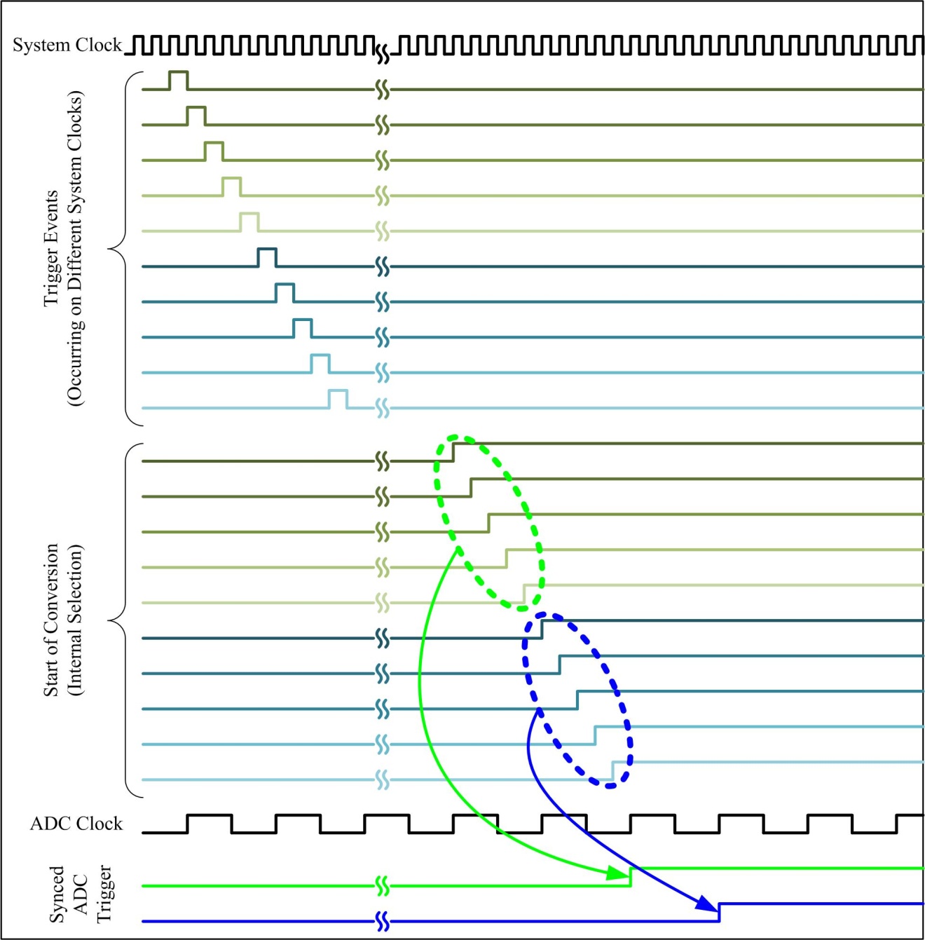
There are four timers in use for signals and sampling (I am using wide timers in 32-bit split-mode):- 

Timer A0 is the PWM test signal.
Timer B0 is a ‘shadow’ timer/signal for triggering, with the same period as the test signal.
Timer A1 triggers the ADC and is pre-loaded with the offset time. This can be a one-shot or periodic timer .
Timer B1 is a one-shot up-counter for timing the ADC conversion time.

Timers A1 and B1 use the wait-for-trigger (daisy-chain) mode to wait on timer B0 to timeout. A1, B1 are configured, pre-loaded, set into wait mode, enabled, and then fire on the next timeout of timer B0. This works very neatly except for a small limitation in daisy-chain mode – a timer must be reset (with ‘peripheral reset’) after each wait-for-trigger, which is a little untidy and will increase the sampling window time.

Using a ‘shadow’ signal (timer B0) with the same period as the PWM test signal means that triggering is guaranteed to occur, for the same offset, on exactly the same 12.5ns tick. If triggering depended instead on a signal on an input pin, then noise introduced onto the signal may introduce jitter.  A second advantage is that the PWM test signal A0 can be moved in precise 12.5ns steps relative to the trigger B0. This is very useful feature for validating the accuracy of results, i.e. the trigger and ADC do not change, and the measured waveform should move by 12.5ns steps (which is demonstrated easily).

An ADC interrupt service routine first records the time B1, then reads the sample. The ‘conversion time’ from the initial trigger (B0 timeout) is then the B1 time plus the timing offset. Only one sample is collected per trigger event B0 for the experiments here (thus A1 in one-shot mode is sufficient).

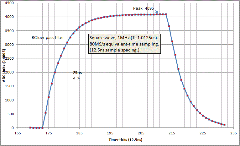
With the MCU at 80MHz (ADC at 16MHz), and trying for 80MS/s, the sample values at a sharp pulse edge (e.g. 10-15ns) seemed to vary rather wildly (which might be expected), but I noticed that the same five values seemed to repeat themselves, and these matched up with the conversion time returned in timer B1.

What appears to happen is that for a fixed offset (12.5ns steps) in timer A1, the conversion time varies over five (12.5ns) steps (obviously 80/16). Recording ADC sample values against conversion time, instead of against time offset in timer A1, shows a highly correlated set of samples (see table below). A narrow, sharply rising/falling pulse is the most demanding test here, as just one tick (12.5ns) of timing jitter would destroy the coherence of the waveform at the transitions. To obtain a uniform distribution of times for one offset (in A1), it helps if a small random delay is added between each sampling event (e.g. using the low ADC bits to add a random delay of a few cycles).

Clearly the switch on the ADC sample-and-hold input circuit must open on a discrete 12.5ns step, and the conversion time returned (via B1) maintains this precision.  Clearly also the interrupt latency (for the ADC ISR), plus any other latencies, are exactly the same every time (though it is possible that some incidental feature or interaction may be maintaining this precise latency, which would be a great shame!). 

However, when the test signal period is a multiple of five timer ticks, only one time is returned, limiting the resolution to 16MS/s. The obvious explanation is that for a fixed offset, successive samples over several test signal cycles do not range over the five steps available inside a 62.5ns (16 MHz) interval, as they do when the period is not divisible by five. (For an external signal, this is less likely to be an issue in general.)

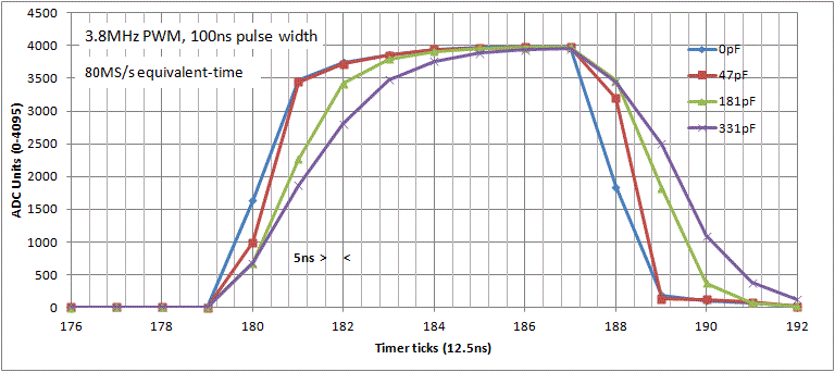
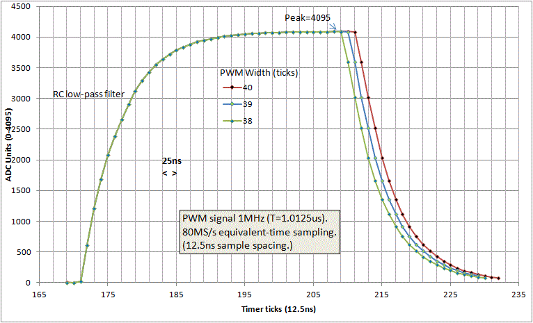
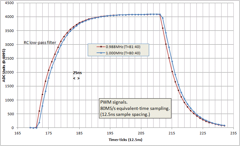
Here are results for 80MS/s equivalent-time sampling, with MCU=80MHz, test signal 3.8MHz PWM, pulse width 100ns (8 ticks at 80MHz), and drive 8mA into a (10R+1.5K) potential divider (to reduce the peak reading below 4095).

Key:

‘Time’ is in timer ticks at 80MHz (12.5ns steps) from signal trigger to sample completed.
 ‘NS’ is the number of samples accumulated for each time (from which the sample mean and rms deviation are computed).
‘Mean’ is the average over ‘NS’ samples (in ADC units 0-4095).
‘Rms’ is the root-mean-square deviation (in ADC units/LSB) from the sample mean (0.5rms is due to digitization).
 
Time   Mean  Rms  NS  ADC Samples (first 12 only)
174    2.5  2.7  34     8    4    1    5    4    4    1    0    5    4    0    0
175    2.6  2.8  51     5    3    0    4    1    4    1    0    5    4    1    1
176    1.5  1.9  64     0    1    0    3    4    4    0    0    5    0    0    5
177    2.3  2.6  64     1    0    2    9    3    0    3    7    1    1    7    3
178    2.3  2.9  64     8    7    7    1    3    2    1    1    1    9    0    0
179    1.8  2.0  57     1    0    3    1    0    3    3    3    5    0    0    5
180 1636.9  9.9  64  1631 1645 1610 1643 1607 1643 1643 1638 1640 1641 1629 1643
181 3467.8  2.1  64  3466 3468 3467 3469 3469 3471 3467 3467 3473 3463 3466 3469
182 3748.3  1.6  64  3747 3748 3748 3749 3749 3749 3748 3746 3749 3748 3747 3749
183 3860.5  1.3  64  3860 3861 3860 3860 3860 3861 3860 3862 3861 3860 3862 3862
184 3942.8  1.1  64  3944 3943 3943 3944 3943 3943 3942 3941 3944 3941 3943 3942
185 3968.2  1.1  64  3967 3970 3968 3970 3969 3969 3970 3968 3967 3970 3968 3968
186 3977.3  1.2  64  3977 3979 3977 3976 3976 3977 3977 3977 3977 3977 3977 3978
187 3980.2  1.1  64  3983 3979 3980 3982 3980 3979 3979 3980 3979 3982 3980 3979
188 1844.7 17.3  64  1868 1842 1866 1832 1854 1846 1866 1823 1842 1864 1806 1836
189  185.9  3.2  64   186  182  186  190  182  190  182  182  182  182  188  182
190  106.3  3.1  64   110  108  106  106  104  110  110  106  108  102  106  103
191   75.1  2.9  64    76   70   76   74   72   75   74   76   76   72   78   78
192   14.5  2.7  64    18   12   15   12   16   12   12   12   14   12   20   16
193    5.6  3.1  64     4    4    5    9    9    9    4   10    8    8    9    4
194    2.9  2.6  64     4    5    0    5    0    0    0    0    4    0    4    0
195    1.3  1.8  64     0    0    1    0    0    0    1    5    0    4    0    4
196    1.5  2.0  64     1    5    1    0    0    0    0    5    0    0    4    0
197    0.7  1.2  64     0    1    0    0    0    0    1    1    0    1    0    1
198    1.7  2.2  64     0    3    2    2    2    0    1    3    0    1    3    1
199    1.7  1.9  59     1    3    6    1    0    0    0    3    0    0    3    2
200    0.9  1.3  64     1    0    1    0    0    0    0    3    3    1    3    0
201 1636.4 10.2  64  1645 1614 1646 1616 1645 1611 1631 1631 1625 1642 1638 1637
202 3468.4  2.5  64  3473 3467 3471 3468 3466 3466 3468 3467 3467 3470 3469 3467
203 3748.5  1.2  64  3748 3750 3749 3748 3747 3749 3748 3747 3747 3748 3748 3748
204 3860.3  1.0  64  3860 3860 3859 3861 3859 3860 3861 3863 3859 3857 3859 3861
205 3942.1  0.7  64  3942 3943 3942 3942 3942 3942 3942 3942 3942 3942 3941 3942
206 3967.8  1.0  64  3967 3968 3967 3969 3967 3967 3967 3969 3969 3967 3967 3967
207 3976.9  0.9  64  3977 3978 3977 3976 3976 3978 3976 3978 3976 3977 3978 3978
208 3980.2  0.7  64  3980 3980 3980 3981 3980 3979 3980 3982 3981 3980 3980 3980
209 1846.5 19.4  64  1848 1824 1838 1848 1826 1857 1836 1836 1856 1847 1836 1860
210  185.1  3.2  64   182  180  180  190  186  190  184  186  182  186  185  182
211  105.2  3.1  64   104  108  110  102  106  104  105  104  108  108  106  107
212   75.0  2.7  64    78   72   78   75   78   78   76   79   76   77   72   78
213   14.0  2.9  64    12   12   12   12    8   12   12   16   21   16   12   12
214    4.5  3.0  64     8    8    4    8    0    5    9    5    5    5    4    5
215    2.2  2.3  64     0    0    0    5    4    4    4    0    0    4    4    4
216    0.8  1.4  64     4    0    0    0    0    0    0    0    1    4    0    0
 
The ‘rms’ column measures the sampling error – this is lowest on signal high, is higher at 0V, and is highest when change is greatest (e.g. at/near the pulse transitions).
Some of this error will be signal variation/noise, some internal ADC noise, some noise picked up along the way, and some may be timing jitter.
The noise on signal high indicates a resolution <0.1% (for rms=1.0, nearly all samples are within +-2 of mean).
For each time, up to 64 samples are collected for averaging - some time slots are sparser than others.

Here is the same PWM pulse (case C=0pF) along with pulses for a range of capacitance values between ADC input and GND :-


The pulse rise/fall times for case C=0pF are in the range 10-15ns (nb. signal into a 1.5K resistance), the data sheet indicates 8-11ns (20% to 80% full-scale).
The trajectory of the waveforms at t=180 suggests that the pulse starts about 5ns before t=180, not at t=179.
Using the case C=331pF, a quick calculation (adding 10pF ADC input capacitance from data sheet) for the rise time (0-3500 in 45ns) gives R=63, and a signal source impedance of 53ohm (i.e. minus 10ohm from the potential divider).

Now a good question is how meaningful are the ADC readings which catch the fastest pulse transitions, i.e. within the range 0-47pF? Rise/fall times of order 10ns would suggest rates of change here of 300V/us. As this is trying to track a change of about 400 ADC units in 1ns, the variation in the samples indicated by the rms value seemed too good to be believable. So, at first glance, I tended to dismiss the readings at the pulse edges, especially since the value returned can be different after a MCU reset (but begging the obvious question, why else should the samples be so consistent?).

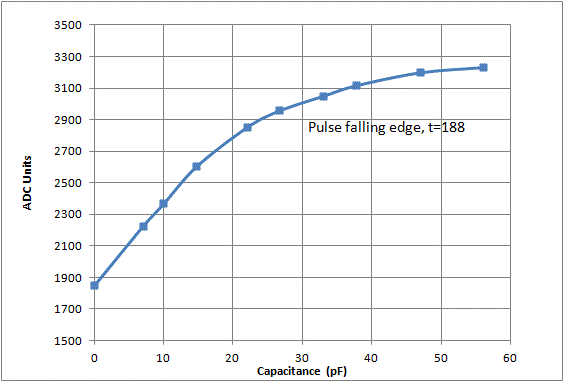
An experiment using low capacitance values (0-47pF) to slow the signal rise and fall times very slightly (e.g. 1ns steps or less) should give distinct and repeatable readings just at the pulse transitions, if there is meaningful resolution available. Here are results using ceramic capacitors between the ADC input and GND for the rising and falling pulse edges (at t=180,188):-


These ADC sample mean values were surprisingly repeatable (e.g. +-2 ADC units) after re-inserting the same capacitor(s) (sometimes a day later!), and the plots show predictable movements. For each C value, the pulse was essentially the same shape (with peak =3980+-2) except at these two times. The rms error from the sample mean at the pulse transitions trends downwards with capacitance (typically 10-20rms for 0pF, 4-7rms for 47pF), the obvious explanation being that the signal rate of change is decreasing.

So this experiment suggests that within a range of about 5ns (see PWM pulse graph for t=180, 188), perhaps ten (and rather more) increments could be resolved, quite easily, by the timer/ADC sub-system, thus indicating a useful 0.5ns resolution. This was very surprising to me, but then I suppose the advantage with this configuration is that the test signal, trigger and the measurement sub-system are highly synchronized (and we have clocks available with a resolution of eight decimal digits!).

The ADC value recorded at a sharp transition seems to be consistent and repeatable after resetting timers, stopping and restarting the test signal and trigger timer (A0, B0) etc.  But after a MCU reset, the transition samples can vary greatly (though resetting the MCU a few times will return eventually to the original values) – this suggests that the timer and/or ADC blocks may synchronize at slightly different points with the (master) PLL after a MCU reset, leading to a slight shift in time which is very obvious at any sharp transitions? (though I would need to look at this further.)

So whilst there is high resolution (<1ns) at sharp transitions, the absolute values there may be less meaningful (though calibration should be possible via a simple circuit to find the position). Anyway, the purpose of this small experiment was simply to estimate the timing resolution, which appears to be very good indeed.

So, the main conclusions are:

Quite high sample timing resolution (<1ns) would seem to be available using the timer and ADC blocks in the configuration outlined.

In general, a single ADC sample (at MCU=80MHz) can range over five distinct values with timing resolution about 50ns. (This is sufficient in many applications, but much higher resolution is possible.)

And some questions/observations:

Does the high sample timing resolution at 80MS/s rely on some incidental feature in the MCU/ADC? (A small modification might lose the data I am relying upon.)

Is there any way around the limit of 16MS/s when the signal period is a multiple of five timer ticks?

Is the behaviour of timer and ADC combination the same in the newer TIVA C MCU’s? (I can verify this later).

The daisy-chain mode timer must be ‘peripheral reset’ before each sample. This will limit the sampling window time. 

Any help/comments would be much appreciated ...

Jim

----


Stellaris LX4F120H5QR, LaunchPad Evaluation Board (EK-LM4F120XL).
DID0: 0x18050003, DID1: 0x1004602c, part marking: 980 YF LX4F120H5QRFIGA3 29C1ZFW G4.
[‘X’ =experimental release, ‘A3’ = revision.]
Stellaris Firmware Development Package, revision 9453.
Code Composer Studio, Version: 5.2.1.00018.

Additional  notes:

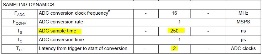
  1. The ADC is clocked using the PLL/25 option (default).
  2. The ADC module ‘sampling rate’ is 1MS/s. This setting is not critical, though lower rates will increase the total sampling window time.
  3. ‘ADC sample phase control’ will divide a 1MS/s interval into 16, so there is less resolution here than using the timer block.
  4. Some results were verified with a second  EK-LM4F120XL board.
  5. The time per sample is 20us. This could be reduced with some optimization, and the daisy-chain timer limitation is an issue.
  6. Occasionally there is an empty time slot at 80MS/s, i.e. with no samples at all. This seems to depend on some internal MCU state.
  7. Shifting the PWM signal in 12.5ns steps (by offsetting timer A0 relative to B0) has been demonstrated.


  • I am just impressed with the detail of this post. So, I will give you 4 stars. Regarding a helpful reply from me, much better to wait for the more experienced people to reply regarding this.

    -kel

  • I am just impressed with the detail of this post. So, I will give you 4 stars. Regarding a helpful reply from me, much better to wait for the more experienced people to reply regarding this.

    I fully agree, an outstanding post. Neither I am an expert on the chip internals ...

    What I'm wondering, how do you handle 80 MS/s without flooding the core ?

  • One further vote to memorialize the effort, care & detail - so evident - your ADC post; but intrudes one huge caution! 

    That said - maker's ADC spec (this from similar LX4F) reveals:

    That "Nominal" 250nS sample time stands in harsh contrast to your findings.  Yet - I've not found a clear, tightly defined "bounding" of that ADC sample time.  (believe that friend Source2 so past requested - this space)   And:

    Where:

    Cadc & Radc enforce (by my calc.) 25nS of "charge/discharge time" which may be further increased by Rs & Cs. To my mind - this casts against the, "80MS/s headline."  Perhaps true - over a very narrowly banded set of conditions - but far too soon, test population (2) too small, (and insufficiently documented - despite this post) for this reporter to support.

    As past suggested - a rapidly ramping, properly bounded, linear signal applied to the ADC may better "prove" such performance claims... (thus the "80MS/s grabber" may not fully meet, "truth in advertising.")

    As always when, "casting far from friendly port" (i.e. this vendor's ADC spec) one must beware of part to part variations - among & between devices, their revisions, device aging and temperature.  (to list a few)  When substantially challenging & exceeding vendor's tech "spec/guidelines" - much caution should be employed.  (do not ask, "how" I know...might uwanted, unanticipated legal exposure be thus invited - overwhelming any/all potential, "ADC gains/savings?")

    Indeed great strides have been made in, "mixed signal" MCU capability - this vendor & others.  Yet - will any dissection of a "pro-grade" scope reveal an MCU as the analog front-end?  Serious ADCs are available from this vendor/others - and to my mind provide a more natural, more robust and far superior analog performance...  After all - that is their, "raison d'etre."

  • I won't even try to catch up with every detail on your magnificent post, but this caught my attention:

    Jim_McCormack said:
    The daisy-chain mode timer must be ‘peripheral reset’ before each sample. This will limit the sampling window time. 

    You probably missed this detail in our earlier timer-trigger thread, but for one-shot mode it's not required to reset the timer peripheral for it to restart counting on the next trigger, re-enabling the timer seems to work fine. See http://e2e.ti.com/support/microcontrollers/tiva_arm/f/908/p/293664/1025833.aspx#1025833

    Also, could you use the "shadow PWM" to trigger the ADC directly? With your current setup the ADC triggering moment seems to be Match_B0 + Match_A1; could you just "include" the A1 offset within Match_B0? Then you would only need one timer to be in wait-for-trigger mode.

    With these changes you should be able to shave off quite a few cycles from everything that needs to be done between two samples.

    BTW, I assume B0 is NOT in PWM mode as you have the triggering working? Errata says a timer in PWM mode won't emit triggers.

  • Thanks all for your comments ...

    fm says >

    What I'm wondering, how do you handle 80 MS/s without flooding the core ?

    Yes, the answer here is that there is a relatively long time between samples. 

    The effective 80MS/s is built up using very fine-grain clocking.

    But if the total sample time is too long, the signal may not be stable within the sampling window.


    Veikko says >

    With these changes you should be able to shave off quite a few cycles from everything that needs to be done between two samples.

    BTW, I assume B0 is NOT in PWM mode as you have the triggering working? Errata says a timer in PWM mode won't emit triggers.

     Thanks for this! I had forgotten that it worked in one-shot, though I fear I recall 'not always'. I will have a look...

    Yes, PWM would not generate a suitable time-out for triggering, though it is better here in any case to use a separate triggering signal of the same period ... B0 is a periodic timer, not PWM.


    cb says >

    That "Nominal" 250nS sample time stands in harsh contrast to your findings

    You are right, cb - the entire 100ns pulse fits within the data sheet 'ADC sample time' of 250ns ! 

    But the voltage 'snapped' by the ADC input circuit will be that when the switch on the sample-and-hold opens.

    I think I recall a paper claiming high-end microwave-range equivalent-time sampling with a 'fairly ordinary' ADC. It is the precise clocking which is the essential bit.

    The proof is 'in the doing' though - is the result sharp and is it consistent? How does it compare with quoted rise/fall times etc.?

    I don't have sufficiently precise test equipment to verify things, but the results I am seeing, in a sense, cannot be explained unless the tracking is very good indeed.

    But, clearly, there is more investigation to do here.

    On the manufacturer's data-sheet figures, some of these seem quite conservative. My simple Launchpad circuit (which is not at all optimized for such an experiment) is clearly getting rather good noise figures for a 100ns PWM signal.


    The exciting thing about these low-cost MCU's for experimenters is their tremendous range of functionality, but also it seems too their relative precision. 

    When I first looked at the LM4F, it was the timer block which drew my attention. I thought, wow!, what could you do with these?

    A small piece of software inside the MCU could offer a surprisingly good self-test/display capability, e.g. of gate-drive signals to a PWM circuit, or a handy 'free' scope with a Launchpad board for experimenters.


    Anyway, thanks for your comments ...

    Jim

    -----


  • Jim,

    There is no way around the 16 MS/s limit.  This is due to the synchronization between the System Clock domain and the ADC clock domain.

    Once the ADC receives a trigger event, the ADC Controller determines if the appropriate conditions have been met to generate a Start of Conversion (SOC) to the ADC.  The Start of Conversion selection is performed in the System Clock Domain.  To initiate the conversion, this signal must be synchronized to the ADC Clock Domain for the ADC.

    As can be seen from the drawing below, a trigger event that will generate a Start of Conversion can be grouped with four neighboring trigger events.  All five of these trigger events will be synchronized to the ADC Clock Domain and result in a Start of Conversion signal that asserts at the exact same time. 


  • @TI Austin,

    Thanks much for your effort in creating this presentation.  (many here felt that, "Ten foot pole rule" was in play - your group.)

    Suspect that Jim may (properly) ask for some explanation/justification for his, "regular, repetitive measurement results" which appear outside of - and in some conflict with - your report here... 

    The, "Start of Conversion" timing has been nicely illustrated (above) but the analysis has not extended into the significance of data sheet's ADC "sample time" (250nS) - might that be of some significance - as well?  (may "torpedo" 16MS/s (sustained) claim)

    Thanks again.

  • Hi Austin,

    Thanks for your reply ... but, following on from poster cb’s comments, I too am unclear, from the information provided, what is happening inside the hardware ...

    Let me approach this from a different angle (and very briefly this time!) ...

    Here is a measurement on a 1MHz square wave with the samples highlighted (red squares). :-

    The signal (internal PWM) has been low-pass filtered to increase the rise and fall times, spreading out the samples to show clearly the step change in measured voltage every 12.5ns sample. The curve closely fits v(t)= 4095 * (1 – exp(-t/RC)) (rise) and v(t) = 4095*exp(-t/RC)) (fall).

    There is good resolution here at 80MS/s (12.5ns) sampling, with low rms variation.

    Now, from what you know of the internal operation of the ADC and timer modules, can you explain how this result comes about? (I have an explanation, but it is necessarily without the benefit of inside knowledge!).

    Thanks,

    Jim

    ----


  • @ Jim,

    Once again - your effort & presentation detail deserve applause.

    Might you clarify - for provider's sake (and those newly arrived, this thread) that your nicely presented curve is in fact synthesized from many program runs - and cannot result from any single, "live ADC run & data-log?"  (i.e. no MCU presently in production is able to acquire & present ADC data - that data acquired @ 12.5nS - continuous intervals)

    Devil in this instance appears centered upon the definition & rigor imposed by, "80MS/s Equivalent, Time Sampling."

    And - continue in the past, expressed belief that a linear, ramping signal avoids the unproductive signal duplication caused by the square wave - and further (perhaps far better) highlights ADC measurement capability @ those 12.5nS intervals...

  • Thanks for your comments cb ... yes, I should repeat for anyone new to this thread :-

    These results are for 'equivalent-time' sampling on a repetitive (periodic) signal, i.e. the waveform is reconstructed by sampling over many cycles.

    (NB. 80MS/s equivalent-time sampling is not possible when the 'signal period is divisible by five', as explained in the original post.)


    Here is another result on PWM signals. The pulse width is reduced in three 12.5ns steps, illustrating an unambiguous 12.5ns resolution:-

    The precise parameters are:-

    Signal PWM:- load: 80, match: 40, width: 40, clk: 80000000
    Signal PWM:- load: 80, match: 41, width: 39, clk: 80000000
    Signal PWM:- load: 80, match: 42, width: 38, clk: 80000000


    Jim

    ----

  • @ Jim,

    Once again - outstanding, detailed presentation - indeed adds to your, "body of ADC evidence."

    Might one more - far more easily acquired - "puzzle piece" make your findings even more compelling?  IMHO a scope capture - showing that same, repetitive signal - superimposed or otherwise "framed" against your, "Equivalent Time Synthesis" plot - would better "correlate" (and thus confirm) that synthesis to your, "real-world, live, signal acquisition."

    Minus this, "missing piece" - no, "exacting" relationship between the actual signal input to the ADC - and that synthesized - has been demonstrated...  (i.e. your synthesis illustrates great, "ADC acquisition data repeatability" - but does not effectively/convincingly tie those ADC (synthetic measurements) to the "real/actual," ADC exciting signal...)

  • [Sorry for the delay in responding, but I like to include something new with any reply...]

    Thanks again cb for your valuable comments ... very true, what I am able to demonstrate is good repeatability and resolution (quantitatively), but for assessing absolute (as opposed to relative) accuracy I have only theoretical prediction to work with (which looks good, but ‘how good’?).

    Unfortunately I am an experimenter with basic equipment including an analog scope which is nowhere near accurate enough. I fear that to prove anything useful, I would need a rather accurate (and expensive) digital scope. On the other hand, in my toolkit, I do have a PhD in EE (RF) from many years back and I do like experimenting! Following on from some of the things you have said, I am next going to synthesize some ‘arbitrary waveforms’ to test against.


    Back to the immediate issue, I have a partial answer to one of my questions ...

    I have discovered a way to measure signals which are a multiple of five clock ticks (MCU=80MHz), e.g. at exactly 1.0MHz (T=80), I was only able to achieve 16MS/s equivalent-time. This is by micro-shifting the signal relative to the timing trigger. Such tampering with the signal may not be permissible/possible in some situations, and it will introduce a transient into what might otherwise be a steady-state signal.

    Timer B is the timing trigger, and PWM timer A is the signal :-

                                    HWREG(WTIMER2_BASE + TIMER_O_TAV) =
    HWREG(WTIMER2_BASE + TIMER_O_TBV) + uOffset ;


    The offset is varied from 0 to 4 inclusive, essentially ‘filling in the gaps’ between the 16MHz ADC clock, and the 80MHz MCU clock. Note that any additional lag in setting timer A like this does not matter so long as the lag is constant, otherwise there will be gaps in the range. These timing changes will mean that the subsequent signal PWM timeout/match will occur slightly sooner or later than expected, usually by only 12.5ns, but more when the offset returns to zero.

    To my surprise, this works quite precisely :-

    (The second curve is shifted by one tick in time simply for comparison.)

    The rms variation is up for the case 1.000MHz, and one might expect that the longer the delay after shifting the signal the lower the variation.

    Jim

    ----